

查询RC4200供应商
RC4200
Analog Multiplier
www.fairchildsemi.com
Features
• High accuracy
• Nonlinearity – 0.1%
Temperature coefficient – 0.005%/°C
• Multiple functions
• Multiply, divide, square, square root, RMS-to-DC
conversion, AGC and modulate/demodulate
• Wide bandwidth – 4 MHz
• Signal-to-noise ratio – 94 dB
Applications
• Low distortion audio modulation circuits
• Voltage-controlled active filters
• Precision oscillators
Description
The RC4200 analog multiplier has complete compensation
for nonlinearity, the primary source of error and distortion.
This multiplier also has three onboard operational amplifiers
designed specifically for use in multiplier logging circuits.
These amplifiers are frequency compensated for optimum
AC response in a logging circuit, the heart of a multiplier,
and can therefore provide superior AC response.
The RC4200 can be used in a wide variety of applications
without sacrificing accuracy. Four-quadrant multiplication,
two-quadrant division, square rooting, squaring and RMS
conversion can all be easily implemented with predictable
accuracy. The nonlinearity compensation is not just trimmed
at a single temperature, it is designed to provide compensation over the full temperature range. This nonlinearity
compensation combined with the low gain and offset drift
inherent in a well-designed monolithic chip provides a very
high accuracy and a low temperature coefficient.
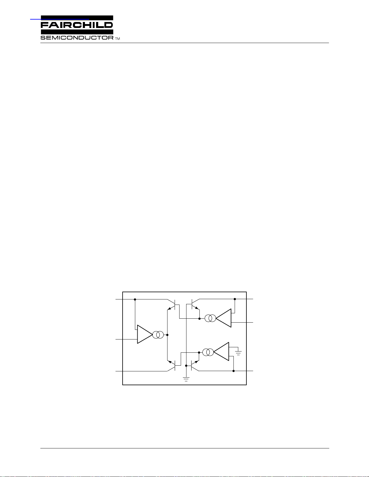
Block Diagram
V
OS2
I
2
–
+
I
3
RC4200
Q2
Q3
Q1
–
+
+
–
Q4
65-4200-01
I
V
I
1
OS1
4
REV. 1.2.1 6/14/01

RC4200 PRODUCT SPECIFICATION
V
BEN
kT
Q
-------
In
I
CN
I
SN
---------
2()=
Functional Description
The RC4200 multiplier is designed to multiply two input
currents (I1 and I2) and to divide by a third input current (I4).
The output is also in the form of a current (I
circuit diagram is shown in the Block Diagram. The nominal
relationship between the three inputs and the output is:
I1I
2
---------
I
3
1()=
I
4
The three input currents must be positive and restricted to a
range of 1 µA to 1 mA. These currents go into the multiplier
chip at op amp summing junctions which are nominally at
zero volts. Therefore, an input voltage can be easily
converted to an input current by a series resistor. Any
number of currents may be summed at the inputs. Depending
on the application, the output current can be converted to a
voltage by an external op amp or used directly. This capabilty of combining input currents and voltages in various
combinations provides great versatility in application.
Inside the multiplier chip, the three op amps make the
collector currents of transistors Q1, Q2 and Q4 equal to their
respective input currents (I
, I2, and I4). These op amps are
1
designed with current source outputs and are phase-compensated for optimum frequency response as a multiplier. Power
drain of the op amps was minimized to prevent the introduction of undesired thermal gradients on the chip. The three op
amps operate on a single supply voltage (nominally -15V)
and total quiescent current drain is less than 4 mA. These
special op amps provide significantly improved performance
in comparison to 741-type op amps.
The actual multiplication is done within the log-antilog
configuration of the Q1-Q4 transistor array. These four
transistors, with associated proprietary circuitry, were
specially designed to precisely implement the relationship.
). A simplified
3
Previous multiplier designs have suffered from an additional
undesired linear term in the above equation; the collector
current times the emitter resistance. The I
term intro-
CrE
duces a parabolic nonlinearity even with matched transistors.
Fairchild Semiconductor has developed a unique and proprietary means of inherently compensating for this undesired
ICrE term. Furthermore, this Fairchild Semiconductor developed circuit technique compensates linearity error over temperature changes. The nonlinearity versus temperature is
significantly improved over earlier designs.
From equation (2) and by assuming equal transistor junction
temperatures, summing base-to-emitter voltage drops around
the transistor array yields:
KT
-------q
In
I
------I
S1
I
1
-------
In
I
S2
I
2
-------
In
I
3
In
––= 0 3()=
S3
I
------I
4
S4
This equation reduces to:
I1I
---------
I3I
The rate of reverse saturation current I
IS1I
--------------IS3I
S2
S4
4()=
S1IS2/IS3IS4
, depends
2
4
on the transistor matching. In a monolithic multiplier this
matching is easily achieved and the rate is very close to
unity, typically 1.0±1%. The final result is the desired
relationship:
I1I
2
---------
I
3
5()=
I
4
The inherent linearity and gain stability combined with low
cost and versatility makes this new circuit ideal for a wide
range of nonlinear functions.
Pin Assignments
I
1
2
V
2
OS2
–V
3
S
I3 (Output)
4
65-4200-07
2 REV. 1.2.1 6/14/01
I
8
1
V
7
OS1
GND
6
I
5
4

PRODUCT SPECIFICATION RC4200
Absolute Maximum Ratings
Parameter Min. Max. Unit
Supply Voltage
1
-22 V
Input Current -5 mA
Storage Temperature Range RC4200/4200A -55 +125 °C
Operating Temperature Range RC4200/4200A 0 +70 °C
Notes:
1. For a supply voltage greater than -22V, the absolute maximum input voltage is equal to the supply voltage.
2. Observe package thermal characteristics.
Thermal Characteristics
(Still air, soldered into PC board)
8-Lead Plastic DIP 8-Lead SOIC
Maximum Junction Temperature +125°C +125˚C
Maximum P
Thermal Resistance θ
Thermal Resistance θ
For TA > 50°C Derate at 6.25mW/°C 4.17mW/˚C
< 50°C 468mW 300mW
D TA
JC
JA
——
160°C/W 240˚C/W
Electrical Characteristics
(Over operating temperature range, VS = -15V unless otherwise noted)
4200A 4200
Parameters Test Conditlons
Total Error as Multiplier TA = +25°C
Untrimmed
With External Trim ±0.2 ±0.2 %
Versus Temperature ±0.005 ±0.005 %/°C
Versus Supply (-9 to -18V) ±0.1 ±0.1 %/V
Nonlinearity
2
50µA ≤ I
1,2,4
≤ 250 µA,
TA = +25°C
Input Current Range
(I1, I2 and I4)
Input Offset Voltage I1 = I2 = I4 = 150 µA
TA = +25°C
Input Bias Current I1 = I2 = I4 = 150 µA
TA = +25°C
Average Input Offset
I1 = I2 = I4 = 150 µA ±50 ±100 µV/°C
Voltage Drift
Output Current Range (I3)
3
Min. Typ. Max. Min. Typ. Max. Units
1
1.0 1000 1.0 1000 µA
1.0 1000 1.0 1000 µA
±2.0 ±3.0 %
±0.1 ±0.3 %
±5.0 ±10 mV
300 500 nA
REV. 1.2.1 6/14/01 3
RC4200 PRODUCT SPECIFICATION
Electrical Characteristics (continued)
(Over operating temperature range, V
Parameters Test Conditlons
Frequency Response,
-3dB point
Supply Voltage -18
Supply Current I1 = I2 = I4 = 150 µA
T
Notes:
1. Refer to Figure 6 for example.
2. The input circuits tend to become unstable at I
(eq. @ I
3. These specifications apply with output (I
be used to drive a resistive load directly. The resistive load should be less than 700Ω and must be pulled up to a positive
supply such that the voltage on pin (4) stays within a range of 0 to +5V.
= I2 = 500 µA, nonlinearity error ≈ 0.5%).
1
= -15V unless otherwise noted)
S
= +25°C
A
, I2, I4 < 50 µA and linearity decreases when I1, I2, I4 > 250 µA
1
) connected to an op amp summing junction. If desired, the output (I3) at pin (4) can
3
4200A 4200
Min. Typ. Max. Min. Typ. Max. Units
4.0
-15 -9.0 -18
4.0
-15 -9.0
MHz
V
4.0 4.0 mA
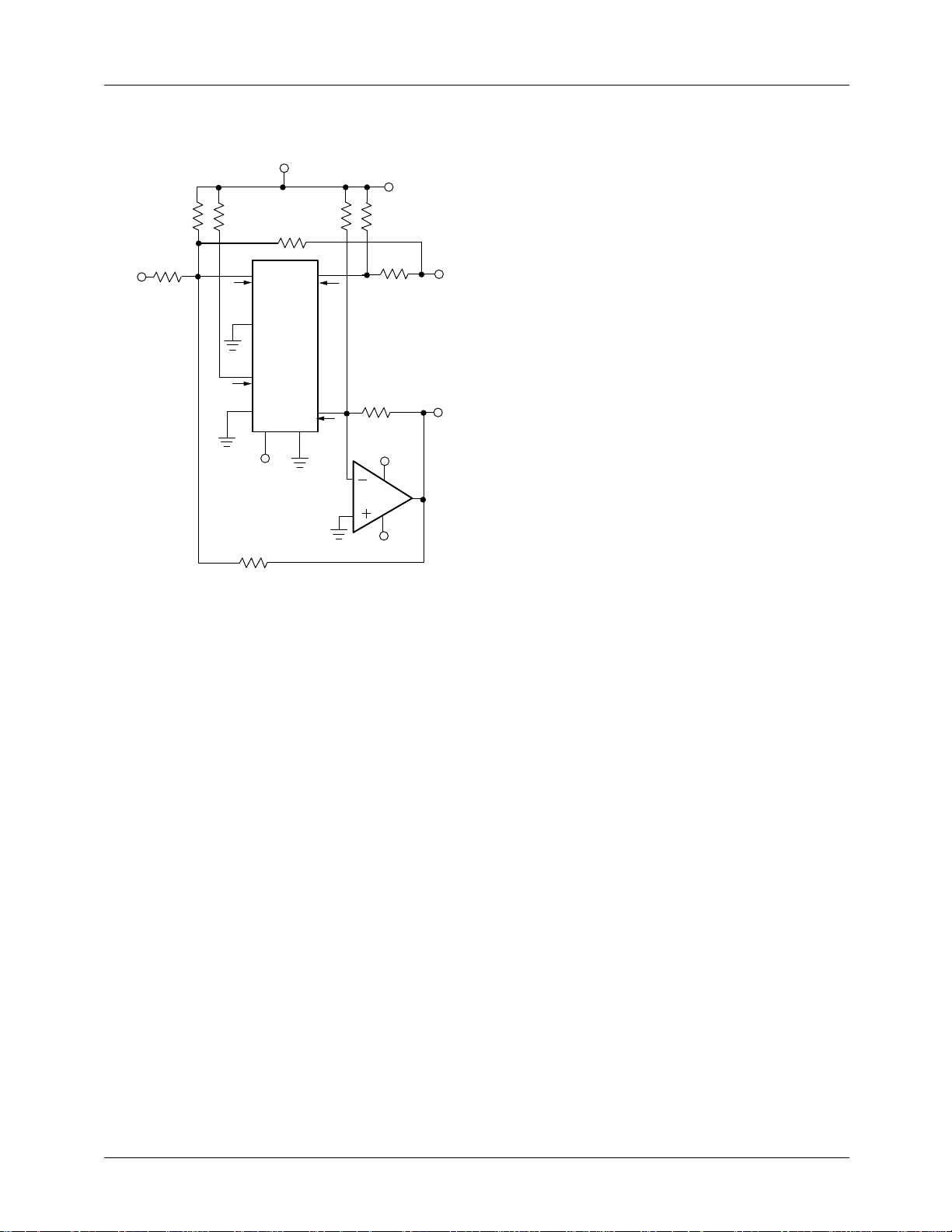
Applications Discussion
Current Multiplier/ Divider
The basic design criteria for all circuit configurations using
the RC4200 multiplier is contained in equation (1), that is,
I1I
I
2
---------=
3
I
4
The current-product-balance equation restates this as:
I1I2I3I4 6()=
R
V
X
1
+
=
I
1
I
V
R
1
X
7
1
RC4200
R
V
Y
2
+
V
I2 =
R
1
I
2
Y
2
2
–V
3
S
Figure 1. Current Multiplier/Divider
58
I
4
V
I4 =
R
Ammeter
4
I
3
6
R
4
+V
Z
Z
4
A
65-4200-02
Dynamic Range and Stability
The precision dynamic range for the RC4200 is from +50
µA
to +250 µA inputs for I1, I2 and I4. Stability and accuracy
degrade if this range is exceeded.
To improve the stability for input currents less than 50 µA,
filter circuits (RSCS) are added to each input (see Figure 2).
R
+V
4
+V
Z
R
S
C
S
R
O
S
–
A1
+
–V
S
V
65-4200-03
O
R
V
X
+
V
Y
R
S
C
S
1
R
C
S
R
2
R
C
S
= 10k Ohms
= 0.005 µF
I
S
1
7
RC4200
1
I
S
2
2
3
–V
S
58
I
4
4
I
3
6
Figure 2. Current Multiplier/Divider with Filters
Amplifier A1 is used to convert the I3 current to an output
voltage.
Multiplier: Vz = constant ≠ 0
Divider: Vy = constant ≠ 0
4 REV. 1.2.1 6/14/01
PRODUCT SPECIFICATION RC4200
VXmin.()VXVX(max.)≤≤
VYmin.()VYVY(max.)≤≤
∆VYVY(max.) = =V
Y
(min.)
Voltage Multiplier/Divider
R
R
V
X
1
I
1
7
4
58
I
4
V
Z
RC4200
R
2
V
Y
VXV
R1R
VOV
Y
=
ROR
2
1
I
2
2
3
–V
Z
4
S
4
V
R
O
I
6
O
3
65-4200-04
Figure 3. Voltage Multiplier/Divider
Solving for V
--------------------------------------=
0
VZ R1R
For a multiplier circuit V
VXVY R0R
Therefore: V
For a divider circuit V
Therefore: V
VXVYK where K
0
Y
V
X
--------
0
K where K
V
Z
Z
4
2
V
R
VRcons ttan==
cons ttan==
R0R
4
---------------------==
VRR1R
V
RR0R4
---------------------==
R1R
2
2
Extended Range
The input and output voltage ranges can be extended to
include 0 and negative voltage signals by adding bias
currents. The RSCS filter circuits are eliminated when the
input and biasing resistors are selected to limit the respective
currents to 50 µA min. and 250 µA max.
Extended Range Multiplier
+V
REF
V
X
(Input)
V
Y
(Input)
R
A
R
1
R
B
I
1
7
RC4200
R
2
1
I
2
2
3
R
C4
–V
R
C
58
I
4
4
I
3
6
S
R
D
V
S
O
(Output)
R
O
+V
Resistors Ra and Rb extend the range of the VX and VY
inputs by picking values such that:
I
min.()
1
and I1(max.)
also I2(min.)
(max.)
and I
2
Resistor R
C
V
X
-----------------------R
VX(max.)
------------------------
V
-----------------------
V
------------------------
supplies bias current for I3 which allows the
V
REF
--------------+ 50 µA,==
R
1
(min.)
R
2
(max.)
R
2
R
a
V
REF
--------------+ 250 µA,==
R
a
V
REF
--------------+ 50 µA,==
R
b
V
REF
--------------+ 250 µA.==
R
b
1
Y
Y
min.()
output to go negative.
Resistors RCX and RCY permit equation (6) to balance, ie.:
V
V
X
--------
R
1
VYV
X
-----------------R1R
2
V0V
REF
------------------------
R0R
V
REF
Y
----------------+
--------
R
R
a
2
VXV
REF
------------------------R1R
b
VXV
REF
-------------------------
RcxR
d
d
VYV
-------------------------
V
REF
----------------+
R
b
REF
R2R
VYV
-------------------------
RCYR
a
REF
V
V
0
=
----------------
-------
R
0
V
REF
----------------
= +++
RaR
b
V
REF
---------------RcR
d
REF
R
C
2
+++
d
------------R
CX
X
Y
-------------+++
R
CY
REF
----------------
R
D
V
V
V
Cross-Product Cancellation
Cross-products are a result of ths V
To the extend that R1Rb = RCXRD, and R2Ra = RCYRd
cross-product cancellation will occur.
XVR
and V
YVR
terms.
Arithmetic Offset Cancellation
The offset caused by the V
extent that RaRb = R0Rd, and the result is:
X
2
V0V
REF
--------------------R0R
d
R0R
d
---------------------------V
REFR1R2
or V0VXVYK==
VYV
---------------R1R
where K =
2
term will cancel to the
REF
Resistor Values
Inputs:
∆VXVX(max.) – =V
V
REF
Constant (+7V to +18V)=
(min.)
X
Figure 4. Extended Range Multiplier
REV. 1.2.1 6/14/01 5
V
R
CX
–V
S
65-4200-05
K
0
---------------VXV
Design Requirements()=
Y
RC4200 PRODUCT SPECIFICATION
R
1
R
a
R
b
R
c
∆V
X
-----------------
, R
200µA
--------------------------------------------------------------------------------=
250µA∆VX200µAVXmax.()–
--------------------------------------------------------------------------------=
250µA∆VY200µAVYmax.()–
RaR
b
-------------
, R
CX
R
d
2
∆VXV
∆VXV
∆V
Y
----------------200µA
REF
REF
R1R
b
------------R
d
, R
, R
d
cy
V
REF
-----------------===
250µA
R2R
a
-------------===
R
d
Multiplying Circuit Offset Adjust
10K ≤ R5 = R9 = R
R
= R
7
R6 = R
R
15
R
8
R
12
R
13
= R14, = 100Ω
11
= 100Ω (VS/0.05)
10
= 100Ω (VS/0.10)
= R1 | | R
= R2 | | R
a
b
= R0 | | RC | | RCX | | R
16
≤ 50K
CY
∆VX∆VYK
R
-----------------------------=
0
160µA
+V
REF
+V
RaR
b
R
–V
1
I
R
6
2
CY
8
R
7
0.1 µF
R
R
10
R
R
R
S
R
1
I
2
12
11 0.1 µF
R
CX
7
1
2
–V
RC4200
3
S
V
X
(Input)
V
Y
(Input)
+V
S
R
X
OS
5
–V
S
+V
S
R
9
Y
OS
6
0.1 µF
R
c
58
I
4
I
3
R
d
100 R
d
R
4
17
R17–R20 can be used to help cancel
crossproduct errors caused by resistor
product mismatch.
R
O
–
R19
R
18
RC5534
+
R
13
+V
S
S
R20 Z
–V
S
VO
(Output)
OS
R16 V
OS
R
R
14
15
–V
S
65-4200-06
Figure 5. Multiplying Circuit Offset Adjust
Procedure
1. Set all trimmer pots to 0V on the wiper.
2. Connect VX input to ground. Put in a full scale square
wave on VY input. Adjust XOS(R5) for no square wave
on V0 output (adjust for 0 feedthrough).
6 REV. 1.2.1 6/14/01
3. Connect VY input to ground. Put in a full scale square
wave on VX input. Adjust YOS(R9) for no square wave
on V0 output (adjust for 0 feedthrough).
4. Connect VX and VY to ground. Adjust VOS(R16) for 0V
on V0 output.
PRODUCT SPECIFICATION RC4200
Extended Range Divider
+V
REF
+V
REF
R
d
R4
4
R
O
+V
S
RC5534
-V
S
65-4200-08
V
V
REF
Z
----------------+
--------
R
R
C
D
4
V
Z
(Output)
V
O
(Output)
V
X
(Input)
R1
R
a
R
b
I
1
I
2
7
RC4200
Multiplier
1
2
-V
R
ao
3
S
R
az
c
58
I
4
I
3
6
R
Figure 6. Extended Range Divider
As with the extended range multiplier, resistors Raz and Rao
are added to cancel the cross-product error caused by the
biasing resistors, i.e.
X
--------
R
1
VXV
REF
------------------------R1R
V0V
Z
----------------
R0R
4
0
----------+
R
ao
b
V0V
-----------------------R0R
Z
---------R
az
V0V
REF
-----------------------RaoR
REF
d
REF
----------------++
R
a
VZV
-------------------------
b
VZV
------------------------R4R
REF
----------------
R
b
REF
RazR
b
V
REF
REF
---------------RcR
c
V
----------------
V
V
V
V
V
V
V
REF
0
----------------+
=
-------
R
R
0
2
REF
=++ +
RaR
b
2
+++
d
To cancel cross-product and arithmetic offset:
Notice that it is necessary to match the above resistor crossproducts to within the amount of error tolerable in the output offset, i.e., with a 10V F.S. output, 0.1% resistor crossproduct match will give 0.1% x 10V. untrimmable output
offset voltage.
Resistor Values
Inputs:
(min.) ≤ VX ≤ VX(max.)
V
X
∆VX = VX(max.) = VX(min.)
VZ(min.) ≤ VZ ≤ VZ(max.)
∆V
= VZ(max.) = VZ(min.)
Z
V
= Constant (+7V to +18V)
REF
Outputs:
V0 (min.) ≤ V0 ≤ V0 (max.)
∆V0 = V0 (max.) = V0 (min.)
V0V
Z
K
R
0
R
c
R
d
R
a
R
1
--------------
Design Requirement()=
V
X
∆V
0
-----------------
, R
750µA
------------------------------------------------------------------------------=
750µA∆V0700µAV0max.()–
-------------------------------------------------------------------------------=
250µA∆VZ200µAVZmax.()–
RcR
------------R
∆V0∆V
----------------------=
600µAK
b
d
, R
az
b
Z
∆V
------------------
∆V0V
∆VXV
RcR
-------------
REF
250µA
REF
REF
4
, R
R
b
, R
ao
4
∆V
Z
-----------------===
200µA
R0R
d
-------------===
R
b
RaoRb = R0Rd, RazRb = R4Rc and RaRb = RcRd
and the result is:
REF
b
V
0VZ
--------------
=
V
----------------------------
or V
R0R
4
REFR0R4
R1R
b
VXV
---------------------R1R
where K =
REV. 1.2.1 6/14/01 7
0
=
V
X
-----------VZK

RC4200 PRODUCT SPECIFICATION
Divider Circuit with Offset Adjustment
+V
REF
R10
R11
R14
R15
R
R16
d
V
Z
+V
S
-V
S
(Input)
S
R13 Z
-V
S
(Output)
R17 V
OS
V (Offset)
O
OS
V (Offset)
Z
V
O
R4
R12
R
O
+V
R
AX
0.1 F
R
c
5
I
4
4
I
3
6
µ
R8
µ
0.1 F
0.1 Fµ
R
b
8
I
1
7
RC4200
Multiplier
1
I
2
2
3
-V
S
R
ao
R
a
X
R1
X
R21 = R
R20
OS
+V
S
V (Offset)
X
R6
R5
R7
-V
S
b
R9
V
(Input)
+V
S
Y
OS
R18
R19
-V
S
R18-R21 can be used in place of R9 to help
cancel gain error due to resistor product
mis-match (See Appendix 1).
General Example: Two-Quad Divider
10K ≤ R
R
R
R
R
R
R
R
R
= R13 = R17 ≤ 50K V0 = K(VX/VZ), K = k, V
5
+ R8 ≈ R1 | | Ra | | Raz | | R
7
≈ R7 (VS/0.05) 0 ≤ VZ ≤ +10, therefore ∆VZ = 20
6
= R
9
b
≈ 100 x R
10
= 20K Rb = 60K R5, R13, R17 = 10K
11
= 100K R4 = 50K R7, R15 = 1K
12
+ R15 ≈ R0 | | R
14
≈ R15 (VS/0.10) Rd = 300K R6, R9, R16 = 300K
16
4
c
ao
-10 ≤ VX ≤ +10, therefore ∆VX = 20
-10 ≤ V0 ≤ +10, therefore ∆V0 = 20
R0 = 26.7K R1 = 333K
Rc = 37.5K R8, R11 = 20K
R
= 187.5K R10 = 4.7M
a
R
= 31.25 R12 = 100K
az
R
= 133K
ao
= +VS = +15V
REF
Figure 7. Divider Circuit with Offset Adjustment
65-1878
8 REV. 1.2.1 6/14/01

PRODUCT SPECIFICATION RC4200
R
1
V0max.()
2
74µ AN
2
----------------------------=
Divider Circuit Offset Adjustment Procedure
1. Set each trimmer pot to 0V on the wiper.
2. Connect VX (input) to ground. Put a DC voltage of
approximatey 1/2 VZ (max.) DC on the VZ (input) with
an AC (squarewave is easiest) voltage of 1/2 VZ (max.)
peak-to-peak superimposed on it. Adjust X
zero feedthrough. (No AC at V0)
V (Max.)
z
1/2 V (Max.)
z
0V
3. Connect V
(input) to VZ (input) and put in the
X
1/2 VZ(max.) DC with an AC of approximately 20 mV
less than VZ(max.).
Adjust Z
1/2 V (Max.)
(R13) for zero feedthrough.
OS
V (Max.)
z
z
0V
4. Return VX (Input) to ground and connect VZ(max.)
DC on VZ(input). Adjust output VOS(R17) for VO =
0V
O
5. Connect VX (input) to VZ (input) and and in VZ (max.)
DC. (The output will equal K.) Decrease the input
slowly until the output (V0 - K) deviates beyond the
desired accuracy. Adjust ZOS to bring it back into tolerance and return to Step 4. Continue steps 4 and 5 until
VZ reduces to the lowest value desired.
Notice that as the input to VX and VZ gets closer to zero (an
illegal state) the system noise will predominate so much that
an integrating voltmeter will be very helpful.
(R5) for
OS
1/2 V (Max.)
z
~
10 mV
~
65-1868
Square Root Circuit V0 = N√VX
+V
REF
c
I
4
3
REF
4
V
-------------------------------
R
d
R4
R
O
+V
S
-V
S
V0V
REF
-----------------------R
R
0
REFR0R4
R1R
b
V
(Output)
65-1877
V
REF
----------------+++=
RcR
d
d
4
R
58
4
3
I
6
V
(Input)
R
R1
X
R
I
b
I
1
2
7
1
2
-V
R
ao
RC4200
Multiplier
S
a
Figure 8.
2
V0V
VXV
-------------------------
If RaRbRcRd and RaoRbR0Rd + RaoRbRcR4RcRdR0R
Then
and V0NVX where N = K=
0VXVXmax.()and V0max.()≤≤ NVXmax.()=
N
RaR
RbR
R
4
R
ao
R
0
V
REF
REF
----------------
R1R
RaR
b
==
2
VXV
V
0
-------------------------
--------------
==
R0R
4
V
0
-------------
Design Requirements()=
V
X
V
REF
----------------==
d
50µ A
V
REF
-----------------==
c
150µ A
V0max.()
------------------------=
50µ A
V0max.()
------------------------=
125µ A
V0max.()
------------------------=
225µ A
b
R1R
------------------------++
RaoR
REF
b
REF
b
or V
V
0
-------------R0R
2
VXK where K =
0
2
4
V0V
-----------------------RcR
O
2
REV. 1.2.1 6/14/01 9

RC4200 PRODUCT SPECIFICATION
R7100Ω=
R
10
R0R
C
||
=
Square Root Circuit Offset Adjust
+V
REF
R10
R11
R12
R
d
R4
R
+V
O
S
-V
S
+V
S
-V
S
R13 V
V
O
(Output)
OS
6
µ
0.1 F
R
c
5
I
4
4
I
3
R8
µ
0.1 F
µ
0.1 F
R
b
8
I
1
RC4200
7
Multiplier
1
I
2
2
3
-V
S
R
ao
R
a
X
R1
R17 = R
R16
+V
S
R6
X
R5
OS
R7
-V
S
b
R9
V
(Input)
+V
S
Y
OS
R14
R15
-V
S
R14-R17 can be used in place of R9 to help
reduce linearity error due to resistor product
mis-match (See Appendix 1).
10K R5≤ R1350K≤=
V
S
----------
R6R
=
R8R1RaR
=
R9Rb=
R
11
R
=
12R11
7
100Ω=
0.05
|| ||
V
-------
0.1
S
65-1876
Figure 9. Square Root Circuit Offset Adjust
Procedure
1. Set both trimmer pots to 0V on the wiper.
2. Put in a full scale (0 to VX(max.) squarewave on VX
input. Adjust XOS(R5) for proper peak-to-peak amplitude on V0 output. (Scaling adjust)
ao
3. Connect VX input to ground. Adjust VOS(R13) for 0V
on V0 output.
10 REV. 1.2.1 6/14/01

PRODUCT SPECIFICATION RC4200
R
c
R
a
2
R
d
------
=
Squaring Circuits V0 = K V
V
X
(Input)
2
V
2VXV
-------R
if R
X
2
1
2
a
REF
------------------------R1R
a
RcRd and R1Ra2RCXR
==
2
V
REF
--------------++
2
R
a
V0V
---------------------
X
R0R
2
REF
d
R1
D
R
a
R1
R
b
I
1
7
Multiplier
1
I
2
2
-V
R
CX
Figure 10. Squaring Circuit
2
V
-------------RcR
REF
VXV
REF
----------------------++=
RcR
d
d
+V
REF
RC4200
3
S
R
c
58
I
4
4
I
3
6
R
R
O
+V
S
RC5534
-V
S
d
V
O
(Output)
65-1875
2
then
V0V
REF
--------------------R0R
d
V
X
--------
or V0KV
==
2
R
1
2
where K =
X
R
0Rd
--------------------V
REFR1
VX(min.) ≤ VX ≤ VX(max.) ∆VX = VX(max.) – VX(min.)
V
0
--------
K
R
R
R
(Design Requirement)=
2
V
X
∆V
X
-----------------
1
200µA
--------------------------------------------------------------------------------
a
250µA∆VX200µAVXmax.()–
-----------------
d
250µA
V
REF
=
=
∆VXV
REF
=
R1R
a
-------------
R
cx
∆V
-------------------
R
0
2R
d
2
X
160µA
=
K
=
2
REV. 1.2.1 6/14/01 11

RC4200 PRODUCT SPECIFICATION
10K R10≤ R1150K≤=
R8, R
15
100Ω=
Squaring Circuits Offset Adjust
+V
REF
+V
S
9100 R
-V
R10 Z
S
OS
V
X
(Input)
RaR
b
R
1
I
R
5
1
7
R
c
58
I
4
R
d
R7 =
d
R
R
8
RC4200
Multiplier
1
I
2
2
3
-V
S
R
14
4
I
3
6
R
16
R
1
V R
OS
0.1 F
R
13
µ
6
0.1 F
R
+V
µ
CX
S
R
-V
S
15
R7-R10 can be used to cancel all
linearity errors caused by input
offsets and resistor product
mis-match (See Appendix 1).
R
O
+V
S
-V
µ
0.1 F
S
V
O
(Output)
65-1874
Figure 11. Squaring Circuit Offset Adjust
R9, R
R5, R
R
16
=
14
R1R
=
6
|| ||
R0RcR
=
100Ω
||
V
-------
0.1
a
S
a
Procedure
1. Set both trimmer pots to 0V on the wiper.
2. Put in a full scale (±VX) squarewave on VX input.
Adjust ZOS(R10) for uniform output.
3. Connect VX input to ground. Adjust VOS(R11) for 0V
on V0 outputs.
12 REV. 1.2.1 6/14/01

PRODUCT SPECIFICATION RC4200
Appendix 1—System Errors
There are four types of accuracy errors which affect overall
system performance. They are:
• Nonimearity—Incremental deviation from absolute
accuracy. See Note 1.
• Scaling Error—Linear deviation from absolute accuracy.
• Output Offset—Constant deviation from absolute
accuracy.
• Feedthrough.—Cross-product errors caused by input
offsets and external circuit limitations. See Note 2.
This nonlinearity error in the transfer function of the
RC4200 is ±0.1% maximum (±0.03 maximum for the
RC4200A). That is,
I1I
I
3
±=
I
4
0.1% F.S.
2
---------
The other system errors are caused by voltage offsets on the
inputs of the RC4200 and can be as high as ±3.0% (±2.0%
for RC4200A).
VXV
----------------
V
0
V
X
V
Y
Notes:
1. The input circuits tend to become unstable at
I
, I2, I4 < 50 µA and linearity decreases when I1, I2, I4 >
1
250 µA (e.g., @ I
2. This section will not deal with feedthrough which is
proportional to frequency of operation and caused by stray
capacitance and/or bandwidth limitations. (refer to
Figure 12.)
3. Not including resistor tolerance or output offset on the
operational amplifier.
4. For 50 µA ≤ I
R0R
Y
-------------
V
R1R
Z
R
1
R
2
1
4()
4
±=
3.0% F.S.
3()4()
2
R
4
R
O
+V
S
Ideal Op-Amp
V = 0
OS
I
I
2
8
1
7
1
2
RC4200
Multiplier
3
-V
S
5
I
4
4
I
3
6
Figure 12.
= I2 = 500µA nonlinearity error ≈ 0.5%).
1
, I2, I4 ≤ 250 µA.
V
Z
V
O
65-1871
Errors Caused by Input Offsets
VXV
R0R
4
V0 =
R0R
4
VY Feedthrough
VX Feedthrough
Scaling Error
Output Offset Error
System errors can be greatly reduced by externally trimming
the input offset voltages of the RC4200. (±3.0% F.S. for
RC4200 and ±0.1% for RC4200A.)
V
X
+V
S
X
OS
-V
S
V
+V
S
-V
S
= X
If X
OS
OSX
Figure 13. RC4200 with Input Offset Adjustment
Y
V
Z
Y
then V
1
VYV
±
V
Z
R
1
R
1
7
R
2
1
R
2
2
, YOS = Y
VXV
----------------
O
V
OSX
RC4200
Multiplier
3
-V
S
OSY
Y
Z
± VXV
OSY
58
4
6
, ZOS = -V
R
0R4
-------------
±0.3% F.S.
R1R
2
± V0V
100 R
OSZ
± V
OSZ
V
R
4
4
R
O
Ideal Op-Amp
V = 0
OS
,
3()
OSXVOSY
Z
+V
S
Z
-V
S
V
O
65-1870
OS
Extended Range Circuit Errors
The extended range configurations have a disadvantage in
that additional accuracy errors may be introduced by resistor
product mismatching.
Multiplier
An error in resistor product matching will cause an
equivalent feedthrough or output offset error. See Figure 6.
R1Rb = RCXRd ±α, VX feedthrough (VY = 0) = IαV
R2Ra = RCYRd ±β, VY feedthrough (VX = 0) = ±βV
RaRb = RCRd ±γ, V0 offset (VX = VY = 0) = ±γV
Note:
* Output offset errors can always be trimmed out with the
output op amp offset adjust, VOS (R16).
REF
X
Y
*
REV. 1.2.1 6/14/01 13

RC4200 PRODUCT SPECIFICATION
Reducing Mismatch Errors
You need not use 0.01% resistors to reduce resistor product
mismatch errors. Here are a couple of ways to obtain
maximum accuracy out of the extended range multiplier
(see Figure 4) using 1% resistors.
Method 1
VX feedthrough, for example, occurs when VY = 0 and
V
≠ 0. This VX feedthrough will equal ±VXV
OSY
Also, if V
V
XVOSZ
feedthrough of ±αV
±V
YVOSX
Total feedthrough:
±VXV
By carefully abusing XOS(R5), YOS(R9) and ZOS(R20) this
equation can be made to very nearly equal zero and the
feedthrough error will practically disappear.
A residual of set will probably remain which can be trimmed
outwith VOS(R16) at the output of amp.
Method 2
Notice that the ratios of R1Rb:RCXRd and R2Ra:RCYRd are
both dependent of Rd also that R1, R2, Ra and Rb are all
functions of the maximum input requirements. By designing
a multiplier for the same input ranges on both VX and V
then R1 = R2, RCX = RCY and Ra = Rb. (Note: it is acceptable to design a four quadrant multiplier and use only two
quadrants of it.)
≠ 0, there is a VX feedthrough equal to
OSZ
. A resistor-product error of α will cause a VX
. Likewise, VY feedthrough errors are:
, ±VYV
OSY ±VYVOSX
X
and ±βV
OSZ
Y
±αVX ±βVY ±(VX + VY) V
OSY
OSZ
Select R
to be 1% or 2% below (or above) the calculated
d
value. This will cause α and β to both be positive (or negative) by nearly the same amount. Now the effective value of
Rd can be trimmed with an offset adjustment ZOS(R20) on
pin 5.
This technique causes: a slight gain error which can be compensated with the R
.
can be trimmed with VOS(R16) on the output op amp.
value, and an output of offset error that
0
Extended Range Divider
The only cross-product error of interest is the VZ
feedthrough (V
= 0 and V
X
≠ 0) which is easily adjusted
OSX
with XOS(R5). See Figure 6.
Resistor product mismatch will cause scaling errors (gain)
that could be a problem for very low values of VZ. Adjustments to YOS(R18) can be made to improve the high gain
accuracy.
Square Root and Squaring
These circuits are functions of single variables so
feedthrough, as such, is not a consideration. Cross product
errors will effect incremental accuracy that can be corrected
YOS(R14) or ZOS(R10). See Figure 9 and Figure 11.
Y
14 REV. 1.2.1 6/14/01

PRODUCT SPECIFICATION RC4200
V
AG
VINtd
0
T
2
---
∫
=
V
rms
for Asinωtdt:
V
rms
A
2
2
------
T
2
---
=
so, |Asinωt|
rms
Asinωt
rms
=
implies V
0
Avg V
IN
2
()=
Appendix 2—Applications
Design Considerations for RMS-to-DC Circuits
Average Value
Consider Vin = Asinωτ. By definition,
Where T = Period
ω = 2πf
2π
------=
T
V
IN
0T2T
T
---
2
2
AG
=
---
∫
T
0
A ωtsin td
V
A
t
65-1873
Therefore, the rms value of Asinωt becomes:
V
rms
RMS Value for Rectified Sine Waves
A
-------=
2
Consider Vin = |A sin ωt|, a rectified wave. To solve,
integrate of each half cycle.
1
---
i.e.
T
1
---
∫
T
This is the same as
2
TV
dt =
in
∫
0
T
---
2
2
sin2ωt dt+ Asinωt–()
A
0
T
T
∫
--2
1
---
TA2sin2ωttd
∫
1
0
2
dt
Practical Consideration: |Asinωt| has high-order harmonics;
Asinωt does not. Therefore, non-ideal integrators may cause
different errors for two approaches.
(a)
2
V
a
IN
Low Pass
Filter
V = V
O
rms
IN
T
2A
1
------T
2A
-------
2π
----
ω
=
Average Value of Asinωt is
RMS Value
--2
ωt cos–
0
π()cos–0()cos+[]=
Again, consider VIN = Asinωt
T
1
V
rms
V
==
AVG
---
∫
T
V
[]2td
IN
0
T
1
2
V
rms
V
rms
V
rms
--T
A
------
A
------
T
2
∫
2
2
A
0
T
∫
0
T
--2
sin2ωt dt
1
--2
1
------4ω
=
=
=
1
---
cos 2 cos 2 ωt–dt
2
T
sin2 ωt–
0
(b)
Absolute
V
IN
2
---
A
π
V
----------
Avg
V
Value
2
IN
0
V
IN
2
a
b
=
V
0
2
V
IN
V
O
Low Pass
Figure 14.
Filter
V = A V
VG
O
65-4200-09
2
IN
V
Avg V
=
0
2
IN
2
A
V
rms
REV. 1.2.1 6/14/01 15
------=
2

RC4200 PRODUCT SPECIFICATION
i.e., V
0
VXV
Y
V
REF
----------------
R0R
d
R1R
2
-------------
=
V
REF
V
H
VY()
∫
==
+V
REF
100K
V
100K
IN
100K
*Determines sacle factor (K) for X function.
**Determines sacle factor (K) for X function.
+V = +V = +15V
REF
s
-V = -15V
s
100K
50K
50K
83.3K
8
7
RC4200A
Multiplier
1
2
36
-V
S
2
45.5 K
100
60K
250K*
RC5532
30K
µ
22 F
1/2
+V
S
10K
-V
S
X
2
0.1 F
167K
5
4
µ
Figure 15. RMS to DC Converter V
300K
13.3K
100K
60K
80K
OUT
10K
8
7
1
2
-V
=√V
RC4200A
Multiplier
X
3
S
0.1 F
2
IN
100K
6
µ
300K
RC5532
30K
200K
44.4K**
1/2
+V
V
OUT
S
10K
-V
S
65-1869
5
4
15K
100
Amplitude Modulator with A.G.C.
In many AC modulator applications, unwanted output
modulation is caused by variations in carrier input amplitude. The versatility of the RC4200 multiplier can be utilizes
to eliminate this undesired fluctuation. The extended range
multiplier circuit (Figure 4) shows an output amplitude
inversely proportional to the reference voltage V
By making V
proportional to VY (where VY is the car-
REF
rier input) such that:
Then the denominator becomes a variable value that automatically provides constant gain, such that the modulating
input (V
) modulates the carrier (VY) with a fixed scale
X
factor even though the carrier varies in amplitude.
REF
.
If VH is made proportional to the average value of Asinωt
(i.e., 2A/π) and scaled by a value of π/2 then:
VH=A
and if: VX = Modulating input (VM)
and: VY Carrier input (Asinωt)
R
0Rd
Then: V0 = K VM sinωt where K =
------------R1R
2
The resistor scaling is determined by the dynamic range of
the carrier variation and modulating input.
The resistor values are solved, as with the other extended
range circuits, in terms of the input voltages.
Input voltages:
Modulation voltage (V
): 0 ≤ VM ≤ VX(max.)
M
Carrier (VY): VY = Asinωt
Carrier amplitude fluctuation (∆A):
A(min.) sint ≤ VY ≤ A(max.) sinΩωt
Dynamic Range (N): A(max.)/A(min.),
A(max.) = VH(max.) and A(min.) = VH(min.)
16 REV. 1.2.1 6/14/01

PRODUCT SPECIFICATION RC4200
RaR
a
R
a
5
R
a
R
O
4
6
µ
0.1 F
C1
p
2
1/4
RC4156
R3 47K
470
V = AVG A sin = A
H
1/4
RC4156
+V
R*
30K
p
2
S
10K
-V
S
t
ω
V =
O
ω
V sin
M
t
A
V
Y
SIN ω
V
M
=
t
+V
10K
+V
10K
R3
30K
S
-V
S
S
-V
R1
R2
R1
R1 R
100
R2 R
100
R3
30K
1/4
RC4156
a
a
R2
1N914
30K
30K
S
R3
30K
µ
0.1 F
µ
0.1 F
8
7
1
2
1/2 R3
RC4200
Multiplier
3
-V
S
15K
1N914
The maximum and minimum values for I
I
(max.)
1
VXmax.()
------------------------R
VHmax.()
-------------------------+ 250µA==
1
R
a
VHmin.()
I1(min.)
I2(max.)
------------------------50µAVMmin.()0== =
R
a
A max.()
---------------------
R
VHmax.()
-------------------------+ 250µA==
2
R
a
VHmin.()
I2(min.)
------------------------50µA==
R
a
For a dynamic range of N, where
A max.()
---------------------
N
A min.()
5,<=
These equations combine to yield:
R
1
R
a
VX(max.)
---------------------------------
5N–()50µA
A(min.)
-------------------
50µA
and R
---------------------------------
, R2
5N–()50µA
= K
O
A(max.)
R1R
2
------------R
a
,=
Figure 16. Amplitude Modulator with A.G.C.
and I2 lead to:
1
Example 1
VY = Asinωt 2.5V ≤ A ≤ 10V, therefore N = 4
0V ≤ VM ≤ 10V, therefore VX(max.) = 10V
K = 1, therefore V0 = VM sinωt
VX(max.)
R
------------------------
1
50µA
A(max.)
R
--------------------
1
50µA
A(min.)
R
-------------------
a
50µA
R
1R2
ROK
------------R
a
Example 2
VY = Asinωt 3 ≤ A ≤ 6, therefore N = 2
0V ≤ VM ≤ 8V, therefore VX(max.) = 8V
K = 0.2, therefore V0 = 0.2 VM sinwt
so:
,=
R1 = 53.3K, R2 = 40K
Ra = 60K and R0 = 7.11K
*R1 R2 Ra R
10V
-------------- 2 0 0 K===
50µA
10V
-------------- 2 0 0 K===
50µA
2.5V
-------------- 5 0 K===
50µA
200K 200 K×
---------------------------------
1
50K
O
65-1866
800K== =
REV. 1.2.1 6/14/01 17

RC4200 PRODUCT SPECIFICATION
Inputs
V
Z
+V
S
V ADJ
OS4
Output
V
X
+V
S
-V
S
V
Y
+V
S
-V
S
R1
50 mV
R2
50 mV
C
C
100
s
100
s
R1
R
s
R
s
V
V
OS1
OS2
I
0.1 F
µ
I
µ
0.1 F
8
1
7
1
2
2
RC4200
Multiplier
3
-V
S
R4
O
R
1/4
4156
0.1 F
100 R4
50 mV
O
Gain
Adj.
µ
5
I
4
4
I
3
V
OS3
6
R
+V
S
-V
S
V
O
XY
V
z
R R4
O
R1 R2
µ
R = 10K, C = 0.005 F
S
Where K =
S
V V
V = K
s
Limited Range, First Quadrant Applications
The following circuit has the advantage that cross-product
errors are due only to input offsets and nonlinearity error is
sightly error is slightly less for lower input currents.
The circuit also has no standby current to add to the noise
content, although the signal-to-noise ratio worsens at very
low input currents (1-5 µA) due to the noise current of the
input stages.
The RSCS filter circuits are added to each input to improve
the stability for input currents below 50 µA.
Caution!
The bandpass drops off significantly for lower currents
(<50 µA) and non-symmetrical rise and fall times can cause
second harmonic distortion.
µ
100 V
-V
S
65-1867
Thermal Symmetry
I
1
2
V
2
Thermal
Symmetry
Line
OS2
–V
Output I
3
S
4
3
The scale factor is sensitive to temperature gradients across
the chip in the lateral direction. Where possible, the package
should be oriented such that forces generating temperature
gradients are located physically on the line of thermal symmetry. This will minimize scale-factor error due to thermal
gradients.
I
8
1
V
7
OS1
GND
6
I
5
4
65-0070
18 REV. 1.2.1 6/14/01

PRODUCT SPECIFICATION RC4200
200 A ac*µ
V
x
µ
150 A dc
µ
250 A dc
V
Y
* Peak to Peak
250 A dcµ
V
x
µ
200 A ac*
V
Y
µ
150 A dc
* Peak to Peak
8
7
1
2
8
7
1
2
-15V
-15V
4200
3
4200
3
6
6
5
4
5
4
µ
250 A dc
µ
250 A dc
+3
V
z
+1
-1
-3
-5
V
o
-7
Relative Output (dB)
-9
-11
10 10210
3
10410
5
10610
65-1863
7
Frequency (Hz)
+3
V
z
+1
-1
-3
V
o
-5
-7
Relative Output (dB)
-9
10
7
65-1864
-11
10 10
2
10
3
10410510
6
Frequency (Hz)
250 A dcµ
V
x
µ
250 A dc
V
Y
* Peak to Peak
8
7
1
2
-15V
4200
3
5
4
6
µ
83.4 A ac*
µ
167 A dc
V
z
V
o
+3
+1
-1
-3
-5
-7
Relative Output (dB)
-9
-11
10 10
2
10
3
10410
5
10610
65-1865
7
Frequency (Hz)
Figure 18. Outputs
REV. 1.2.1 6/14/01 19

RC4200 PRODUCT SPECIFICATION
300
250
200
µ
( A)
1
150
I
100
1.0 nA
50
1.2 nA
50 100 150 200 250 300
I2 ( A)µ
Figure 19a. Output Noise Current (I
vs. Input Currents (I
, I2) for I4 = 250µA vs. Input Currents (I4, I1) for I2 = 250µA
1
250
P-P
200
150
250
5 nA
4 nA
3 nA
2.5 nA
µ
( A)
4
I
200
150
100
2 nA
3 nA
4 nA
2 nA
1.5 nA
) Figure 19b. Output Noise Current (I3)
3
65-1861
50
50
100
150
I1 ( A)
µ
Multiplier Configuration
V V
X
V =
o
Y
10
5 nA
200
6 nA
7 nA
9 nA
11 nA
15 nA
25 nA
65-1862
250
V = 0
100
50
AC Feedthrough (mV )
0
1.0
10 100 1K 10K
Y
V = 10 sin t
X
ω
V = 0
X
V = 10 sin t
Y
ω
100K
65-1860
1M
Frequency (Hz)
Figure 20. AC Feedthrough vs. Frequency
20 REV. 1.2.1 6/14/01

PRODUCT SPECIFICATION RC4200
Mechanical Dimensions
8-Lead SOIC Package
Symbol
A .053 .069 1.35 1.75
A1 .004 .010 0.10 0.25
B .013 0.33
C .008 .010 0.20 0.25
D .189 .197 4.80 5.00
E .150 .158 3.81 4.01
e
H
h
L .016 .050 0.40 1.27
N8 8
α
ccc .004 0.10——
85
Inches
Min. Max. Min. Max.
.020 0.51
.050 BSC 1.27 BSC
.228 .244 5.79 6.20
.010 .020 0.25 0.50
0° 8° 0° 8°
EH
Millimeters
Notes
Notes:
1.
Dimensioning and tolerancing per ANSI Y14.5M-1982.
2.
"D" and "E" do not include mold flash. Mold flash or
protrusions shall not exceed .010 inch (0.25mm).
3.
"L" is the length of terminal for soldering to a substrate.
4.
5
2
2
3
6
Terminal numbers are shown for reference only.
5.
"C" dimension does not include solder finish thickness.
6.
Symbol "N" is the maximum number of terminals.
14
D
A
e
B
A1
SEATING
PLANE
– C –
LEAD COPLANARITY
ccc C
h x 45°
C
α
L
REV. 1.2.1 6/14/01 21

RC4200 PRODUCT SPECIFICATION
Mechanical Dimensions (continued)
8-Lead Plastic DIP Package
Symbol
A — .210 — 5.33
A1 .015 — .38 —
A2 .115 .195 2.93 4.95
B .014 .36
B1 .045 .070 1.14 1.78
C .008 .015 .20 .38
D .348 .430 8.84 10.92
D1
E
E1
e
eB
L
N
E1
Inches
Min. Max. Min. Max.
.022 .56
.005 — .13 —
.300 .325 7.62 8.26
.240 .280 6.10 7.11
.100 BSC 2.54 BSC
— .430 — 10.92
.115 .160 2.92 4.06
8° 8° 5
D
4
1
Millimeters
Notes
4
2
2
Notes:
1.
Dimensioning and tolerancing per ANSI Y14.5M-1982.
2.
"D" and "E1" do not include mold flashing. Mold flash or protrusions
shall not exceed .010 inch (0.25mm).
3.
Terminal numbers are for reference only.
4.
"C" dimension does not include solder finish thickness.
5.
Symbol "N" is the maximum number of terminals.
5
D1
A
A1
B1
8
e
A2
L
B
E
C
eB
22 REV. 1.2.1 6/14/01

RC4200 PRODUCT SPECIFICATION
Ordering Information
Part Number Package Operating Temperature Range
RC4200N 8-Lead Plastic DIP 0°C to +70°C
RC4200AN 8-Lead Plastic DIP 0°C to +70°C
RC4200M 8-Lead SOIC 0°C to +70°C
RC4200AM 8-Lead SOIC 0°C to +70°C
DISCLAIMER
FAIRCHILD SEMICONDUCTOR RESERVES THE RIGHT TO MAKE CHANGES WITHOUT FURTHER NOTICE TO
ANY PRODUCTS HEREIN TO IMPROVE RELIABILITY, FUNCTION OR DESIGN. FAIRCHILD DOES NOT ASSUME
ANY LIABILITY ARISING OUT OF THE APPLICATION OR USE OF ANY PRODUCT OR CIRCUIT DESCRIBED HEREIN;
NEITHER DOES IT CONVEY ANY LICENSE UNDER ITS PATENT RIGHTS, NOR THE RIGHTS OF OTHERS.
LIFE SUPPORT POLICY
FAIRCHILD’S PRODUCTS ARE NOT AUTHORIZED FOR USE AS CRITICAL COMPONENTS IN LIFE SUPPORT DEVICES
OR SYSTEMS WITHOUT THE EXPRESS WRITTEN APPROVAL OF THE PRESIDENT OF FAIRCHILD SEMICONDUCTOR
CORPORATION. As used herein:
1. Life support devices or systems are devices or systems
which, (a) are intended for surgical implant into the body,
or (b) support or sustain life, and (c) whose failure to
perform when properly used in accordance with
instructions for use provided in the labeling, can be
reasonably expected to result in a significant injury of the
user.
2. A critical component in any component of a life support
device or system whose failure to perform can be
reasonably expected to cause the failure of the life support
device or system, or to affect its safety or effectiveness.
www.fairchildsemi.com
6/14/01 0.0m 003
© 2001 Fairchild Semiconductor Corporation
Stock#DS30004841
 Loading...