

Page 1
RC4194
Dual Tracking Voltage Regulators
Features
www.fairchildsemi.com
• Simultaneously adjustable outputs with one resistor
to ±42V
• Load current – ±200 mA with 0.04% load regulation
Description
The RC/RM4194 are dual polarity tracking regulators
designed to provide balanced or unbalanced positive and
negative output voltages at currents to 200 mA.
A single external resistor adjustment can be used to change
both outputs between the limits of ±50 mV and ±42V.
These devices are designed for local “on-card” regulation,
eliminating distribution problems associated with singlepoint regulation. To simplify application the regulators
require a minimum number of external parts.
The device is available in three package types to accommodate various power requirements. The K (TO-66) power
package can dissipate up to 3W at T
14-pin dual in-line will dissipate up to 1W and the N
14-pin dual in-line will dissipate up to 625 mW.
= +25°C. The D
A
• Internal thermal shutdown at T
• External balance for ±V
unbalancing
OUT
• 3W power dissipations
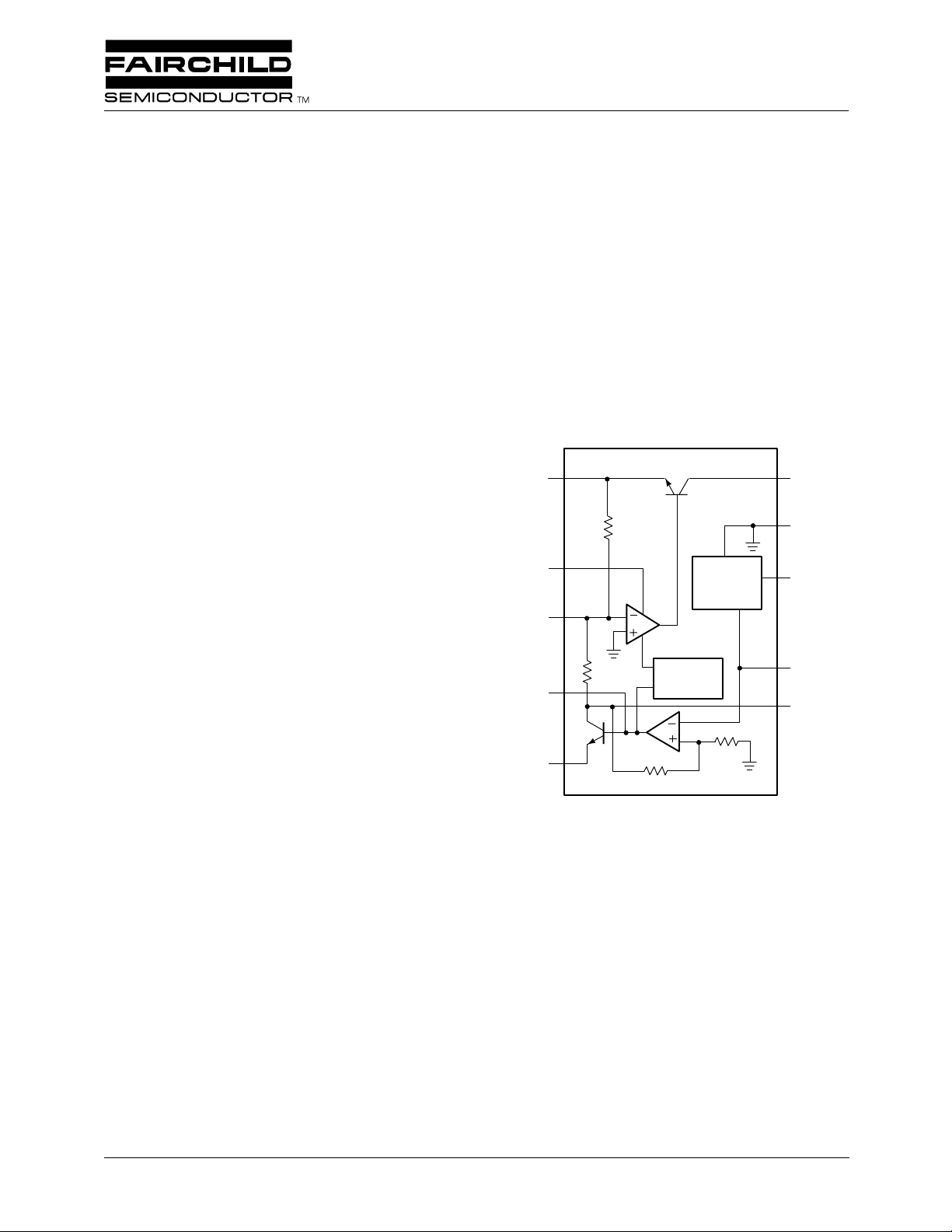
Block Diagram
4194
+V
OUT
20K
Comp+
Bal
20K
Comp–
Thermal
Shutdown
= +175°C
J
100µA
Current
Source
+V
GND
R
SET
R
O
–V
S
OUT
–V
S
3R
R
65-4194-01
Rev. 1.0.0
Page 2
PRODUCT SPECIFICATION RC4194
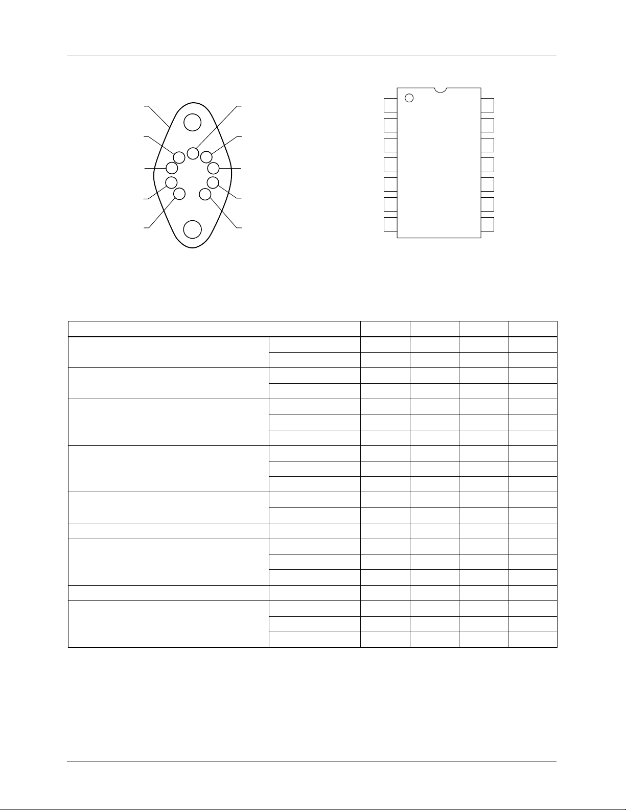
Pin Assignments
+V
-V (Case)
S
+V
OUT
Comp+
Comp-
Bal
+V
S
GND
5
4
6
7
8
9
3
2
1
R
SET
R
O
-V
OUT
65-4194-02
OUT
NC
Comp+
Bal
Comp-
NC
-V
1
2
3
4
5
6
S
7
14
13
12
11
10
9
8
65-4194-03
Absolute Maximum Ratings
(beyond which the device may be damaged)
Parameter Min Typ Max Units
Supply Voltage RC4194 ±35 V
Supply Input to Output Voltage Differential RC4194 ±35 V
Load Current PDIP 100 mA
< 50°C PDIP 468 mW
P
DTA
Operating Temperature (Tj) RC4194 0 70 °C
Storage Temperature -65 150 °C
Junction Temperature PDIP 125 °C
Lead Soldering Temperature (60 seconds) 300 °C
For TA > 50°C Derate at TO-66 Metal Can 23.81 mW/°C
Note:
1. Functional operation under any of these conditions is NOT implied.
1
RM4194 ±45 V
RM4194 ±45 V
CerDIP 150 mA
TO-66 Metal Can 250 mA
CerDIP 1042 mW
TO-66 Metal Can 2381 mW
RM4194 -55 125 °C
CerDIP 175 °C
TO-66 Metal Can 150 °C
PDIP 6.25 mW/°C
CerDIP 8.38 mW/°C
+V
NC
GND
R
SET
R
O
NC
-V
OUT
S
2
Page 3
RC4194 PRODUCT SPECIFICATION
Operating Conditions
Parameter Min Typ Max Units
q
JC
Thermal Resistance CerDIP 60 °C/W
TO-66 Metal Can 7 °C/W
q
JA
Thermal Resistance PDIP 160 °C/W
CerDIP 120 °C/W
TO-66 Metal Can 42 °C/W
Electrical Characteristics
(±5 £ V
unless otherwise specified)
Parameters Test Conditions Min Typ Max Units
Line Regulation DV
Load Regulation
Output Voltage Drift With
Temperature
Positive Output V
Negative Output V
Supply Current3 (Positive) VS = ±V
Supply Current4 (Negative) VS = ±V
Supply Voltage RM4194 ±9.5 ±45 V
Output Voltage Scale Factor R
Output Voltage Range RM4194: R
Output Voltage Tracking ±0.4 ±2.0 %
Ripple Rejection F = 120 Hz, Tj = +25°C70dB
Input-Output Voltage Differential IL = 50 mA, Tj = +25°C 3.0 V
Short Circuit Current VS = ±30V, Tj = +25°C 300 mA
Output Noise Voltage CL = 4.7 mF, V
Internal Thermal Shutdown 175 °C
Notes:
1. Measured as (mA)
2. Output voltage temperature drift guaranteed by design.
3. The current drain will increase by 50mA/V
4. The specifications above apply for the given junction temperatures since pulse test conditions are used.
OUT
£ V
; –VIN £ -8V; IL = ±1mA; RM4194: -55°C £ Tj £ +125°C; RC4194: 0°C £ Tj £ +70°C
MAX
1
2
DV
OUT
æö
------------------
èø
V
OUT
§
100%´
I
L
= 0.1 V
S
IN
4194K: IL < 200 mA
4194D: IL < 100 mA
±VS = ± (V
= ±5V 0.002 0.015 %/°C
OUT
= ±5V 0.003 0.015 %/°C
OUT
MAX
OUT
, V
+ 5)V
OUT
= 0V,
0.04 0.1 %V
0.002 0.004 %V
OUT/IL
(mA)
+0.8 +2.5 mA
IL = 0 mA
, V
MAX
OUT
= 0V,
-1.8 -4.0 mA
IL = 0 mA
RC4194 ±9.5 ±35 V
= 71.5 kW, Tj = +25°C,
SET
VS = ±V
MAX
= 71.5 kW,
SET
2.38 2.5 2.62 kW/V
0.05 ±42 V
IL = 25 mA
RC4194: R
= 71.5 kW,
SET
0.05 ±42 V
IL = 25 mA
OUT
= ±15V,
250 mV
F = 10 Hz to 100 kHz
on positive side and 100mA/V
OUT
on negative side.
OUT
OUT
RMS
3
Page 4
PRODUCT SPECIFICATION RC4194
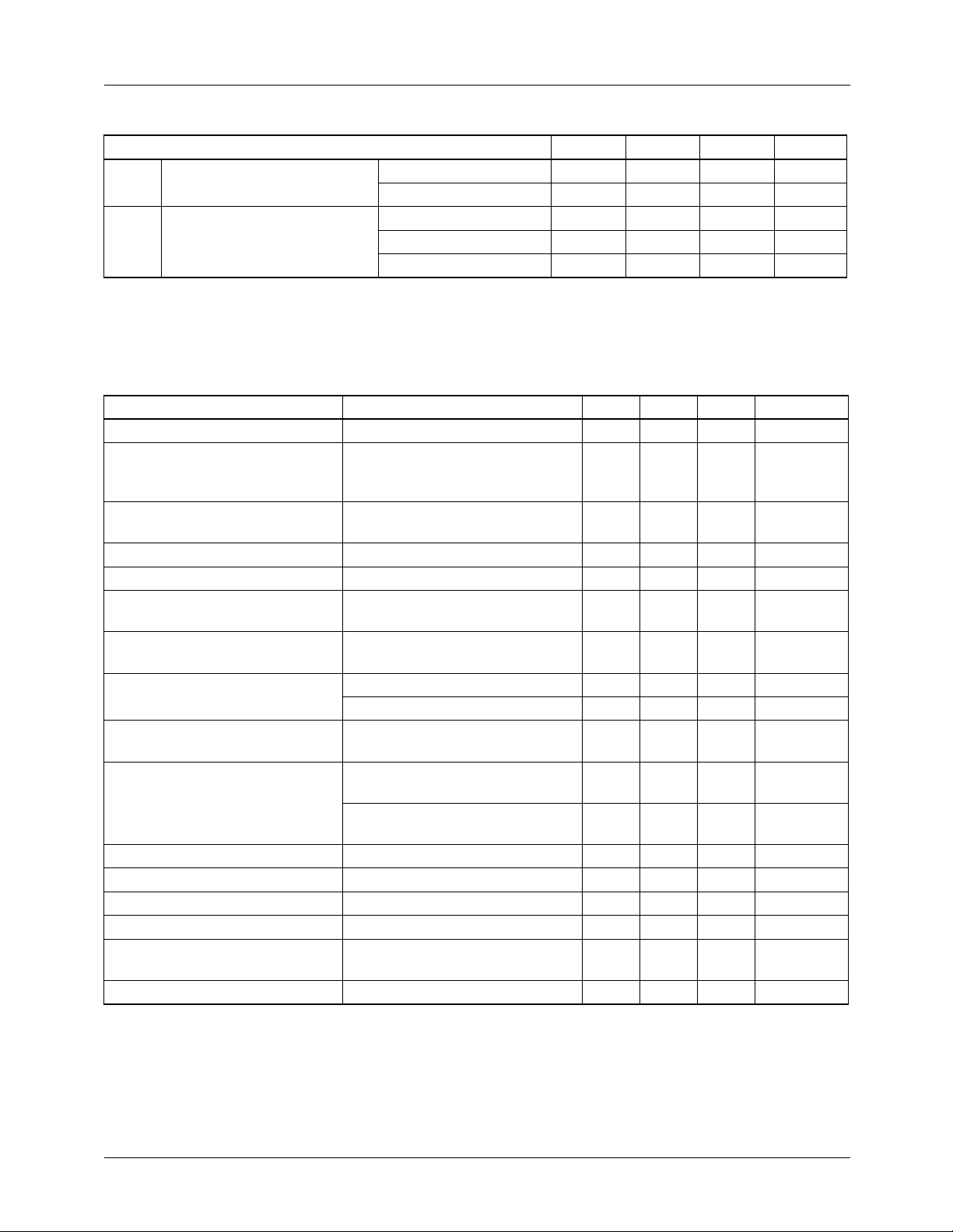
Typical Performance Characteristics
150
130
110
90
70
50
Ripple Rejection (dB)
30
10
0 100 1K 10K 100K
V
OUT
= ±15V
F (Hz)
65-0201
0.06
)
L
0.05
/I
OUT
0.04
0.03
0.02
0.01
0
Load Regulation (% V
-0.01
0
20 40 60 80
100
I
(mA)
L
Tj = +125¡C
T
= +25¡C
j
120 140 160
180
65-0202
200
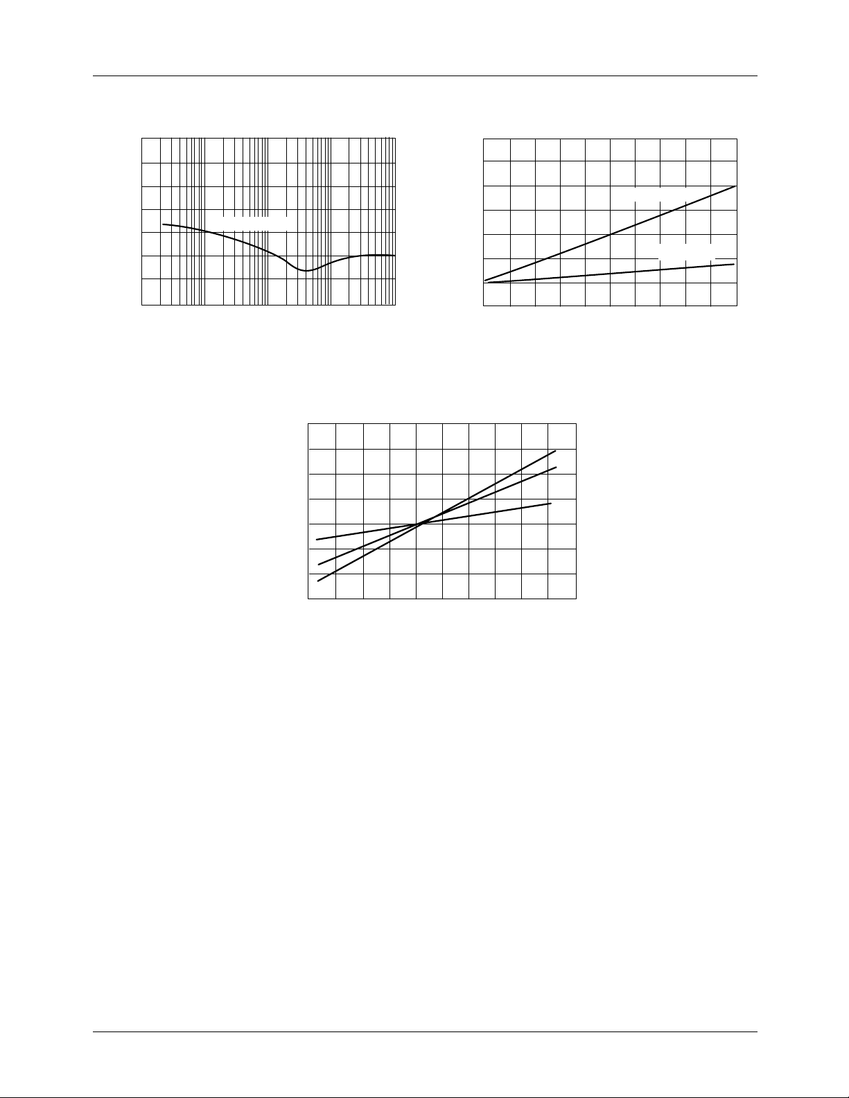
Figure 1. Ripple Rejection vs. Frequency Figure 2. Load Regulation vs. Load Current
)
0.8
OUT
0.6
0.4
0.2
-0.2
0
A
B
-0.4
C
-0.6
Output Voltage Tracking (% V
-60
-40
-20 0
+20 +40 +60 +80+100
+120+140
65-0203
T
(¡C)
j
A = % Tracking of V
B = T.C. for Positive Regulator
OUT
C = T.C. for Negative Regulator
Figure 3. Output Voltage Tracking vs. Temperature
4
Page 5
RC4194 PRODUCT SPECIFICATION
Typical Applications
+V
4.7µF**
OUT
To Additional
Comparators
0.01µF
+V
S
+V
Comp+
S
+V
OUT
R
A
RM4194
-V
S
-V
S
R
Comp-
SET
Gnd
R
Bal
R
-V
0
OUT
B
4805
71.5K
R
0
(Typically 15 RC4805s)
-V = -5V
OUT
To Additional
Comparators
4.7µF
65-0205
0.01µF
R (k½ ) = 2.5 (-V )
O
Adjust R for -V = -5V (12.5 k )
R = R = 20 k½ (See Schematic)
F2
F1
+ V = -V
OUT
R = when +V -V
A
R = when +V -V
B
For +V = 5 when -V = -5V
OUT
R =
A
R =
B
OUT
OUT
O
R R
F1 A
OUT
R R
F2
OUT
OUT
OUT
B
W
OUT
OUT
Figure 4. Unbalanced Output Voltage — Comparator Application
R *
SC
+V
OUT
60µF**
+V
2N4905 or equiv.
m
0.1 F
2N2297 or equiv.
W
S
47
+V
GND
S
Comp+
+V
OUT
4194
W
-V
S
47
2N2297 or equiv.
R *
SC
m
0.1 F
-V
S
71.5K
Comp-
R
SET
R
0
2N914 or equiv.
*R =
**Optional usage - Not as critical as -V bypass capacitors.
0.7
SC
I
SC
O
Note: Compensation and bypass capacitor connections should be close as posibe to the 4194
Figure 5. High Output Application
-V
OUT
-V
OUT
60µF
R
0
Load regulation
10 mV @ 2.5A
R (k ) = 2.5 V
W
O
O
65-0206
5
Page 6

PRODUCT SPECIFICATION RC4194
Typical Applications (continued)
+V = +15V
OUT
To Additional
0.001µF
+V
S
-V
S
71.5K
4.7µF**
Comp+
+V
S
4194
-V
S
R
Comp-
SET
Gnd
+V
OUT
741
-V
R
OUT
0
R
0
-V = -15V
4.7µF
Op Amps
(Typically 180 741s)
OUT
To Additional
Op Amps
0.001µF
65-0204
R (k½) = 2.5 V
O
OUT
Figure 6. Balanced Output Voltage — Op Amp Application
+V = +25V
S
2
In
6
Out
REF-02
Gnd
4
4.87K
15
1
Ref+
Ref-
V
LC
R2
250
-V
S
C
C
14
316
Comp
-V
S
DAC-08
B1
567891011 12
MSB
Binary Inputs
0.01µF
13
+V
B8
S
I
O
I
O
LSB
V = 4 I R1
0.001
I
O
4
75
Comp
2
R
0
+V
RC4194K
S
+V
6
O
OUT
O
+V (0 to +19.92V)
10µF
OUT
R1
2.49K
2
NC
3
R
SET
Comp-+-V
9
S
Case 4
-V
Gnd
1
O
-V (0 to -19.92V)
OUT
10µF
0.001
-V = -25V
S
Adjust R2 for -19.92V at -V
then optionally adjust R3 for +19.92V at +V
65-1725
with all "1s" at binary inputs,
OUT
OUT
RC4194K
Optional Tracking
6
+V
o
100K
8
Bal
1
-V
o
Adjustment
R3
100K
Figure 7. Digitally Controlled Dual 200 mA Voltage Regulator
6
Page 7

RC4194 PRODUCT SPECIFICATION
RC4194 Switchable Power Supply
The outputs of the RC4194 can be simultaneously switched
on or off under logic control as shown in Figure 8. In the
“off” state, the outputs will be forced to a minimum voltage,
or about ±20 mV, rather than becoming open-circuit. The
turn-on time, with the outputs programmed to ±12V, is
approximately 200 mS. This circuit works by forcing the R0
pin to ground with an analog switch.
Refer to the RC4194 internal schematic diagram. A reference voltage that regulates with respect to –VS is generated
at the RSET pin by the zener diode Q12 and the buffer circuit of Q11 and Q13. When the external 71.5k RSET resistor is connected between the R
current of 100 mA is generated which then flows into Q13’s
collector. Since Q13’s collector is tied to the R0 pin, the 100
mA current will develop a ground-referenced voltage drop
proportional to the value of R0, which is then amplified by
the internal error amplifier. When the analog switch in Figure 8 turns on, it effectively shorts out R0 and causes 0V to
be applied to the error amplifier. The output voltage in the
off state will be approxi-mately ±20 mV. If a higher value
(50 to 100 mV) is acceptable, then the DG201 analog switch
can be replaced with a low-cost small signal transistor, as
shown in the alternate switch configuration.
pin and –VS, a precision
SET
Compensation
For most applications, the following compensation technique
is sufficient. The positiv e re gulator section of the RC4194 is
compensated by a 0.001 mF ceramic disc capacitor from the
Comp+ terminal to ground. The negative regulator requires
compensation at two points. The first is the Comp– pin,
which should have 0.001 mF to the –VS pin, or case. A
ceramic disc is ideal here. The second compen-sation point
for the negative side is the –V
should be a 4.7 mF solid tantalum capacitor with enough
reserve voltage capacity to avoid the momentary shorting
and reforming which can occur with tantalum caps. For systems where the cost of a solid tantalum capacitor cannot be
justified, it is usually sufficient to use an aluminum capacitor
with a 0.03 mF ceramic disc in parallel to bypass high frequencies. In addition, if the rectifier filter capacitors have
poor high frequency characteristics (like aluminum electrolytics) or if any impedance is in series with the +V
terminals, it is necessary to bypass these two points with
0.01 mF ceramic disc capacitors. Just as with monolithic op
amps, some applications may not require these bypass caps,
but if in doubt, be sure to include them.
terminal, which ideally
OUT
and –VS
S
+V
S
0.001 F
-V
S
Logic
*Quad SPST CMOS Analog Switch
+V
R
SET
71.5K
S
DG201
–V
Gnd
C
0.001 µF
+V
S
Comp–
m
–V
S
R
SET
S
*
4194
R
0
R
30K
0
Comp+
Gnd
+V
–V
OUT
4.7 µF
OUT
4.7 µF
* Alternate Switch Configuration
47K
4194
+12V
-12V
2N3904
R
0
30K
65-4083
Figure 8. ±12V Switchable Power Supply
7
Page 8

PRODUCT SPECIFICATION RC4194
All compensation and bypass caps should have short leads,
solid grounds, and be located as close to the 4194 as possi-
0.001µF
ble. Refer to Figure 9 for recommended compensation circuitry.
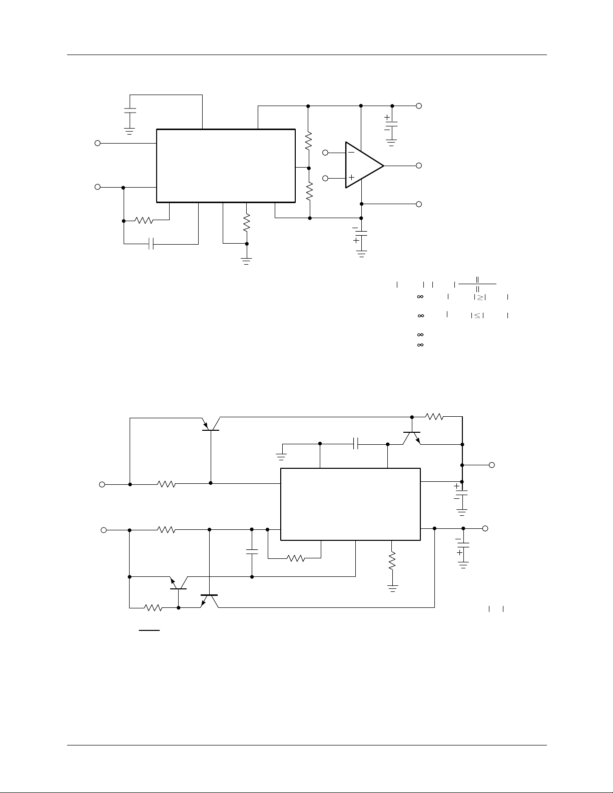
Protection
In systems using monolithic voltage regulators, a number of
conditions can exist which, left uncorrected, will destroy the
regulator. Fortunately, regulators can easily be protected
against these potentially destructive conditions. Monolithic
regulators can be destroyed by any rev ersal of input or output
+V
–V
S
0.01µF
S
+V
–V
R
Comp+
4194
R
SET
+V
OUT
–V
OUT
Comp-
4.7µF
*
S
S
R
0
R
0
SET
voltage polarity, or if the input voltage drops below the output voltage in magnitude. These conditions can be caused by
0.001µF
inductive loads at the inputs or outputs of the regulator.
Other problems are caused by heavy loads at the unregulated
inputs to the regulator, which might cause the input voltage
to drop below the output voltage at turn-off. If any of the
preceding problem conditions are present in your system, it
0.01µF
Note:
All Capacitors are Ceramic Disc
Except * = Solid Tantalum
is recommended that you protect the regulator using diodes.
These diodes should be high speed types capable of handling
Figure 9. RC4194 Recommended Compensation
large current surges. Figure 10 shows all six of the possible
protection diodes. The diodes at the inputs and outputs prevent voltages at those points from becoming reversed.
Diodes from outputs to inputs prevent the output voltage
from exceeding the input voltage. Chances are that the system under consideration will not require all six diodes, but if
in doubt, be sure to include them.
Sometimes occasions arise in which the RC4194 ratings
must be exceeded. One example is the “brownout.” During
a brownout, line voltages may be reduced to as low as 75
VRMS, causing the input voltage to the RC4194 to drop
below the minimum dropout voltage. When this happens,
the negative output v oltage can go to positiv e. The maximum
amount of current available is approximately 5 mA.
Brownout Protection
The RC4194 is one of the most easily applied and troublefree monolithic ICs available. When used within the data
sheet ratings (package power dissipation, maximum output
current, minimum and maximum input voltages) it provides
In general this is not enough current to damage most ICs
which the RC4194 might be supplying, but it is a potentially
destructive condition. Fortunately, it is easy to protect
against. As sho wn in the typical application circuit in Figure
11, a diode, D, can be connected to the negative output.
the most cost-effective source of regulated ±15V for powering linear ICs.
+V
OUT
–V
OUT
65-4201
0.001µF
+V
S
0.01µF
-V
S
To
-V
OUT
+V
-V
R
0.01µF
Comp+
S
4194
R
S
0
R
0
SET
+V
OUT
-V
Comp-
0.001 F
OUT
4.7µF
*
R
SET
Note:
All Capacitors are Ceramic Disc
Except * = Solid Tantalum
-V
65-4202
+V
OUT
OUT
Figure 10. RC4194 Regulator Showing All Protective Diodes
8
Page 9

RC4194 PRODUCT SPECIFICATION
TJTAPDq
JA–
+=
VINV
OUT
–()IOVINIQ´+´=
If a small signal silicon diode is used, it will clamp the negative output voltage at about +0.55V. A Schottky barrier or
germanium device would clamp the voltage at about +0.3V.
Another cure which will keep the negative output ne gati v e at
all times is the 1 mW resistor connected between the +15V
output and the Comp- terminal. This resistor will then supply drive to the negative output transistor, causing it to saturate to -1V during the brownout.
Heatsinking
Voltage Regulators are power devices which are used in a
wide range of applications.
When operating these devices near their extremes of load
current, ambient temperature and input-output differential,
consideration of package dissipation becomes important to
avoid thermal shutdown at 175°C. The RC4194 has this feature to prevent damage to the device. It typically starts
affecting load regulation approximately 2°C below 175°C.
T o av oid shutdown, some form of heatsinking should be used
or one of the above operating conditions would need to be
derated.*
The following is the basic equation for junction temperature:
Equation 1
where
Let’s look at an application where a user is trying to deter-
mine whether the RC4194 in a high temperature environ-
ment will need a heatsink.
Given:
TJ at thermal shutdown = 150°C
TA = 125°C
q
= 41.6°C/W, K (TO-66) pkg.
J-A
VIN = 40V
V
= 30V
OUT
IQ = 1 mA + 75 mA/V
OUT
x 30V
= 3.25 mA*
q
P
Solve for I
I
TJTA–
------------------=
JA–
D
O
I
O
P
TJTA–
------------------=
q
JA–
O
------------------------------------------------ -
q
JA–VINVOUT
150°C 125°C–
-----------------------------------------
41.6°C/W 10V´
D
,
TJTA–
–()
40 3.25´ 103–´
--------------------------------------- -–=
V
´
INIQ
-----------------------------------–=
V
–()
INVOUT
10
TJ = junction temperature (°C)
TA = ambient air temperature (°C)
PD = power dissipated by device (W)
q
= thermal resistance from junction to ambient
J-A
air (°C/W)
The power dissipated by the voltage regulator can be detailed
as follows:
P
VINV
D
Equation 2
–()IOVINIQ´+´=
OUT
where
VIN = input voltage
V
= regulated output voltage
OUT
IO = load current
IQ = quiescent current drain
———————————————
*The current drain will increase by 50mA/V
on positive side and 100mA/V
OUT
= 60 mA – 13 mA ~ 47 mA
If this supply current does not provide at least a 10% margin
under worst case load conditions, heatsinking should be
employed. If reliability is of prime importance, the multiple
regulator approach should be considered.
In Equation 1, q
can be broken into the following compo-
J-A
nents:
q
= q
+ q
J-A
J-C
C-S
+ q
S-A
where
q
= junction-to-case thermal resistance
J-C
q
= case-to-heatsink thermal resistance
C-S
q
= heatsink-to-ambient thermal resistance
S-A
on negative side
OUT
9
Page 10

PRODUCT SPECIFICATION RC4194
In the above example, let’s say that the user’s load current is
200 mA and he wants to calculate the combined q
q
he needs:
S-A
C-S
and
Given: IO = 200 mA,
–()IOVINIQ´+´
INVOUT
50°C 125°C–
TJTA–
3–
´´
q
---------------------------------------------------------------------------=
JA–
V
--------------------------------------------------------------------------------- -=
10V 200mA´ 40+ 3.25 10
Given q
q
C-S
= 7.15°C/W for the 4194 in the K package,
J-C
+ q
= 11.75°C/W – 7.15°C/W
S-A
= 4.6°C/W
When using heatsink compound with a metal-to-metal
interface, a typical q
The remaining q
= 0.5°C/W for the K package.
C-S
of approximately 4°C/W is a large
S-A
enough thermal resistance to be easily provided by a number
of heatsinks currently available. Table 1 is a brief selection
guide to heatsink manufacturers.
= 11.75°C/W
Table 1. Commercial Heatsink Selection Guide
No attempt has been made to provide a complete list of all heatsink manufacturers. This list is only representative.
1
q
(°C/W) Manufacturer/Series or Part Number
S-A
TO-66 Package
0.31 – 1.0 Thermalloy — 6441, 6443, 6450, 6470, 6560, 6590, 6660, 6690
1.0 – 3.0 Wakefield — 641
Thermalloy — 6123, 6135, 6169, 6306, 6401, 6403, 6421, 6423, 6427, 6442, 6463, 6500
3.0 – 5.0 Wakefield — 621, 623
5.0 – 7.0 Wakefield — 690
7.0 – 10.0 Wakefield — 672
10.0 – 25.0 Thermalloy — 6-13, 6014, 6015, 6103, 6104, 6105, 6117
20 Thermalloy — 6007
30 Thermalloy — 6010
32 Thermalloy — 6011
34 Thermalloy — 6012
45 IERC — LI
60 Wakefield — 650, 651
Staver Co., Inc.: 41-51 N Saxon Ave., Bay Shore, NY 11706
IERC: 135 W Magnolia Blvd., Burbank, CA 91502
Thermalloy: P.O. Box 34829, 2021 W Valley View Ln., Dallas, TX
Wakefield Engin Ind: Wakefield, MA 01880
* All values are typical as given by manufacturer or as determined from characteristic curves supplied by manufacturer.
Thermalloy — 6606, 6129, 6141, 6303
IERC — HP
Staver — V3-3-2
Thermalloy — 6002, 6003, 6004, 6005, 6052, 6053, 6054, 6176, 6301
IERC — LB
Staver— V3-5-2
Thermalloy — 6001, 6016, 6051, 6105, 6601
IERC — LA, uP
Staver — V1-3, V1-5, V3-3, V3-5, V3-7
Dual In-line Package
10
Page 11

RC4194 PRODUCT SPECIFICATION
Simplified Schematic Diagram
(7)
Comp+
+V
OUT
-V
s
(5)
1.1
3000
Q42
Q36
R21
R20
Q36
200
Q41
R19
Q40
Q38
Q35
(6)
R23
RF1
20K
(8)
Bal
R24
Q37
RF2
20K
(4)
Q31
Q44
R8
Gnd
5000
Q20
Q16
R9
15K
Q21
Q17
Q45
(1)
-V
Q25
OUT
Q26
Q27
8 kW
Q24
Q19
200W
Q46
Q18 Q43
Q22
R15
R14
W
1.1
W
3000
R10
1650
65-0198
(9)
Comp-
S
-V
To Case
Q30
Q28
Q32
Q33
Q29
Q34
R18
10K
Q47
R5
R4
Q1
25K
500
Q3
Q7
Q10
Q9
Q13
Q4
Q11
Q2
C1
Q12
R6
10 pF
R1
30K
12K
Q8
Q6
Q23
Q5
R7
R3
R11
5000
5000
R2
3900
680
(2)
R
SET 0
(3)
R
Note: Pin numbers are for K package.
11
Page 12

PRODUCT SPECIFICATION RC4194
Mechanical Dimensions
9-Lead Metal Can IC Header Package
øD
øD1
A
øb
S
e1
e
F
øp
r2
Symbol
A .250 .340 6.35 8.64
øb .028 .034 .71 .86
øD — .620 — 15.75
øD1 .470 .500 11.94 12.70
e
e1
F .050 .075 1.27 1.91
øp
q
r1
r2
S
Notes:
1. All leads—increase maximum limit by .003 (.08mm) when
lead finish is applied.
Inches
Min. Max. Min. Max.
.190 .210 4.83 5.33
.093 .107 2.36 2.72
.360 — 9.14 —
.142 .152 3.61 3.86
.958 .962 24.33 24.43
— .350 — 8.89
— .145 — 3.68
.570 .590 14.48 14.99
Millimeters
Notes
1
r1
q
12
Page 13

RC4194 PRODUCT SPECIFICATION
Mechanical Dimensions (continued)
14-Lead Ceramic DIP Package
Symbol
A — .200 — 5.08
b1 .014 .023 .36 .58
b2 .045 1.14
c1 .008 .015 .20 .38
D — .785 — 19.94
E .220 .310 5.59 7.87
e
eA
L .125 .200 3.18 5.08
Q
s1
a
E
s1
Inches
Min. Max. Min. Max.
.065 1.65
.100 BSC 2.54 BSC
.300 BSC 7.62 BSC
.015 .060 .38 1.52
.005 — .13 —
90¡ 105¡ 90¡ 105¡
7
8
Millimeters
D
1
14
Notes
8
2
8
4
4
5, 9
7
3
6
NOTE 1
Notes:
1.
Index area: a notch or a pin one identification mark shall be located
adjacent to pin one. The manufacturer's identification shall not be
used as pin one identification mark.
2.
The minimum limit for dimension "b2" may be .023 (.58mm) for leads
number 1, 7, 8 and 14 only.
3.
Dimension "Q" shall be measured from the seating plane to the base
plane.
4.
This dimension allows for off-center lid, meniscus and glass overrun.
5.
The basic pin spacing is .100 (2.54mm) between centerlines. Each
pin centerline shall be located within ±.010 (.25mm) of its exact
longitudinal position relative to pins 1 and 14.
6.
Applies to all four corners (leads number 1, 7, 8, and 14).
7.
"eA" shall be measured at the center of the lead bends or at the
centerline of the leads when "a" is 90¡.
8.
All leads – Increase maximum limit by .003 (.08mm) measured at the
center of the flat, when lead finish applied.
9.
Twelve spaces.
e
A
Q
b2
L
b1
eA
a
c1
13
Page 14

PRODUCT SPECIFICATION RC4194
Mechanical Dimensions (continued)
14-Lead Plastic DIP Package
Symbol
A — .210 — 5.33
A1 .015 — .38 —
A2 .115 2.93
B .014 .36
B1 .045 .070 1.14 1.78
C .008 .015 .20 .38
D .725 .795 18.42 20.19
D1 .005 — .13 —
E
E1
e
eB — .430 — 10.92
L
N
E1
Inches
Min. Max. Min. Max.
.195 4.95
.022 .56
.300 .325 7.62 8.26
.240 .280 6.10 7.11
.100 BSC 2.54 BSC
.115 .200 2.92 5.08
14 14 5
D
7
Millimeters
1
Notes
4
2
2
Notes:
1.
Dimensioning and tolerancing per ANSI Y14.5M-1982.
2.
"D" and "E1" do not include mold flashing. Mold flash or protrusions
shall not exceed .010 inch (0.25mm).
3.
Terminal numbers are shown for reference only.
4.
"C" dimension does not include solder finish thickness.
5.
Symbol "N" is the maximum number of terminals.
8
D1
e
A
A1
B1
14
E
C
L
B
eB
14
Page 15

PRODUCT SPECIFICATION RC4194
Ordering Information
Product Number Temperature Range Screening Package SMD Number
RC4194N 0° to +70°C Commercial 14 pin Plastic DIP
RC4194D 0° to +70°C Commercial 14 pin Ceramic DIP
RC4194K 0° to +70°C Commercial 9 pin TO-66
RM4194D -55°C to +125°C Commercial 14 pin Ceramic DIP
RM4194D/883B -55°C to +125°C Military 14 pin Ceramic DIP 7705401CA
RM4194K -55°C to +125°C Commercial 9 pin TO-66
Note:
1./883B suffix denotes MIL-STD-883, Par. 1.2.1 compliant device.
LIFE SUPPORT POLICY
FAIRCHILD’S PRODUCTS ARE NOT AUTHORIZED FOR USE AS CRITICAL COMPONENTS IN LIFE SUPPORT DEVICES
OR SYSTEMS WITHOUT THE EXPRESS WRITTEN APPROVAL OF THE PRESIDENT OF FAIRCHILD SEMICONDUCTOR
CORPORATION. As used herein:
1.Life support devices or systems are devices or systems
which, (a) are intended for surgical implant into the body,
or (b) support or sustain life, and (c) whose failure to
perform when properly used in accordance with
instructions for use provided in the labeling, can be
reasonably expected to result in a significant injury of the
user.
2.A critical component in any component of a life support
device or system whose failure to perform can be
reasonably expected to cause the failure of the life support
device or system, or to affect its safety or effectiveness.
www.fairchildsemi.com
5/20/98 0.0m 001
Ó 1998 Fairchild Semiconductor Corporation
Stock#DS30004194
 Loading...