Fairchild QVE11233 service manual

QVE11233 — Sloted Optical Switch
July 2011
QVE11233
Sloted Optical Switch
Features
■
Lead spacing 0.300”
Gap width of 0.150”
■
■
Printed circuit board mounting
2mm aperture width
■
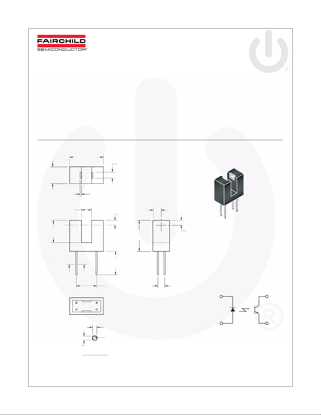
Package Dimensions
0.50 (12.70)
0.25 (6.35)
0.15 (3.81)
0.331 (8.38)
+
E
0.03 (0.76)
2 PLCS
Description
The QVE11233 is designed to allow the user maximum
flexibility in applications. Each switch consists of an
infrared emitting diode facing an NPN phototransistor
across a 0.150” (3.81mm) gap.
0.08 (2.03)
S
+
2 PLCS
0.71 (1.78)
C
L
0.46 (11.68)
0.125±0.005
(3.18)
C
L
0.071 (1.78)
0.35 (8.89) MIN
X
X
2
1
.020 (.50)
3
4
SECTION X-X
0.30 (7.62)
.020 (.50)
.03 (.75)
.023 (.60)
PIN 1 ANODE
PIN 2 CATHODE
PIN 3 COLLECTOR
PIN 4 EMITTER
0.10 (2.54)
Schematic
2
1
3
4
Notes:
1. Dimensions for all drawings are in inches (millimeters).
2. Tolerance of ± 0.010 (0.25) on all non-nominal dimensions unless otherwise specified.
©2011 Fairchild Semiconductor Corporation www.fairchildsemi.com
QVE11233 Rev. 1.1.0

QVE11233 — Sloted Optical Switch
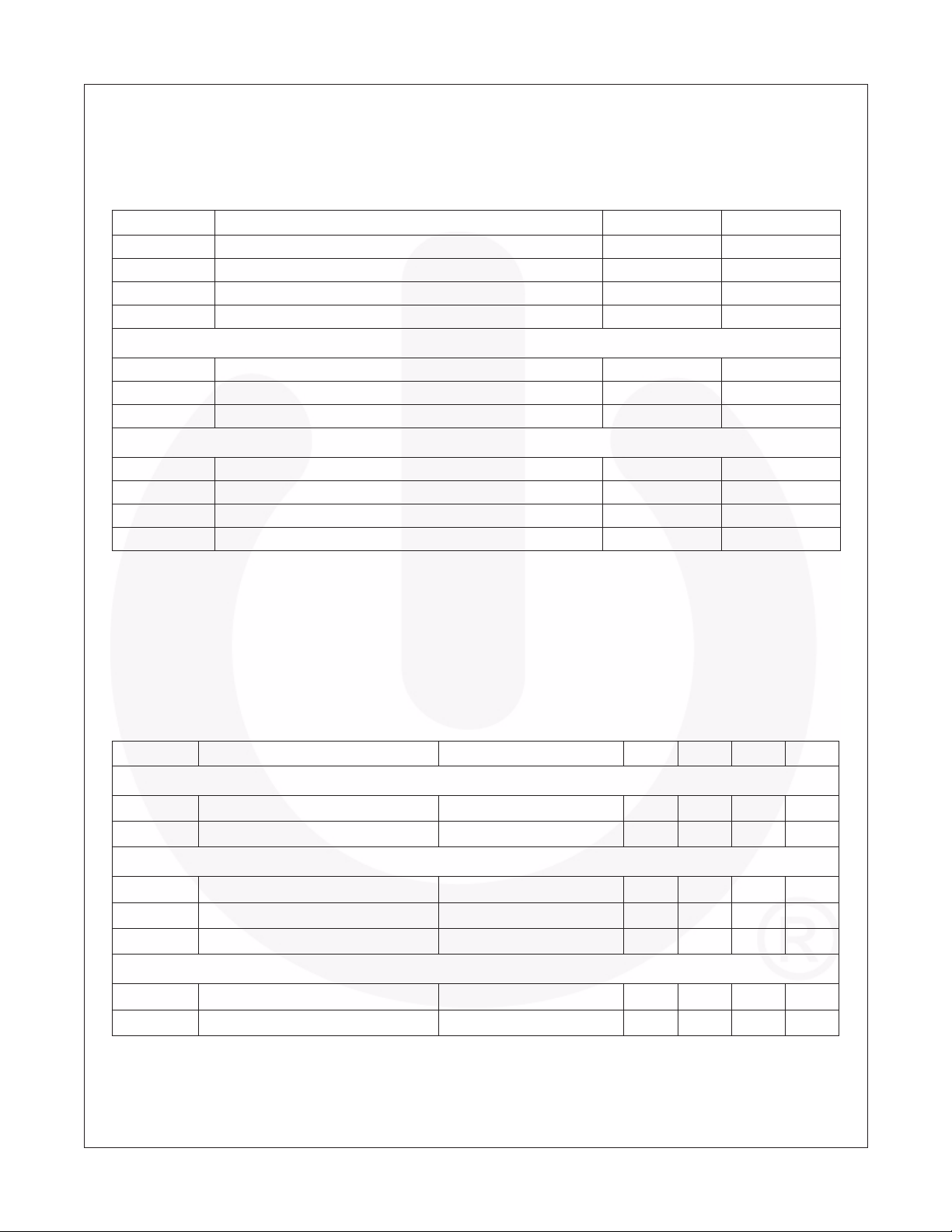
Absolute Maximum Ratings
A
(T
= 25°C unless otherwise specified)
Stresses exceeding the absolute maximum ratings may damage the device. The device may not function or be
operable above the recommended operating conditions and stressing the parts to these levels is not recommended.
In addition, extended exposure to stresses above the recommended operating conditions may affect device reliability.
The absolute maximum ratings are stress ratings only.
Symbol Parameter Rating Units
T
OPR
T
STG
T
SOL-I
T
SOL-F
INPUT (EMITTER)
I
F
V
R
P
D
OUTPUT (SENSOR)
V
CEO
V
ECO
I
C
P
D
Notes:
1. Derate power dissipation linearly, on each component, 1.67mW/°C above 25°C.
2. RMA flux is recommended.
3. Methanol or isopropyl alcohols are recommended as cleaning agents.
4. Soldering iron tip 1/16” (1.6mm) from housing.
Operating Temperature -40 to +85 °C
Storage Temperature -40 to +85 °C
Soldering Temperature (Iron)
Soldering Temperature (Flow)
(2)(3)(4)
(2)(4)
240 for 5 sec °C
260 for 10 sec °C
Continuous Forward Current 50 mA
Reverse Voltage 6 V
Power Dissipation
(1)
100 mW
Collector to Emitter Voltage 30 V
Emitter to Collector Voltage 4.5 V
Collector Current 20 mA
Power Dissipation
(1)
150 mW
Electrical/Optical Characteristics
(T
A
= 25°C)
Symbol Parameter Test Conditions Min. Typ. Max. Units
INPUT (EMITTER)
V
I
R
OUTPUT (SENSOR)
BV
ECO
BV
CEO
I
CEO
COUPLED
I
C(ON)
V
CE (SAT)
©2011 Fairchild Semiconductor Corporation www.fairchildsemi.com
QVE11233 Rev. 1.1.0 2
Forward Voltage I
F
Reverse Leakage Current V
Emitter to Collector Breakdown I
Collector to Emitter Breakdown I
Collector to Emitter Leakage V
On-State Collector Current I
Saturation Voltage I
= 20mA 1.7 V
F
= 2V 100 µA
R
= 100µA, E
E
= 1mA, E
C
= 10V, E
CE
= 20mA, V
F
= 20mA, I
F
= 0 5.0 V
e
= 0 30 V
e
= 0 100 nA
e
= 5V 0.5 mA
CE
= 0.25mA 0.40 V
C
 Loading...