Fairchild QVE00033 service manual

QVE00033 — Phototransistor Optical Surface Mount Interrupter Switch
November 2010
QVE00033
Phototransistor Optical Surface Mount Interrupter Switch
Features
■
No contact switching
Transistor Output
■
■
Compact surface mount package
Opaque black plastic housing
■
■
2mm wide slot
0.4 mm aperture width
■
■
Tape and reel
■
Reflow conditions:
Preheat = 160°C for 120 seconds
Reflow = 200°C for 60 seconds (peak = 240°C)
■
HL-94V-0 housing
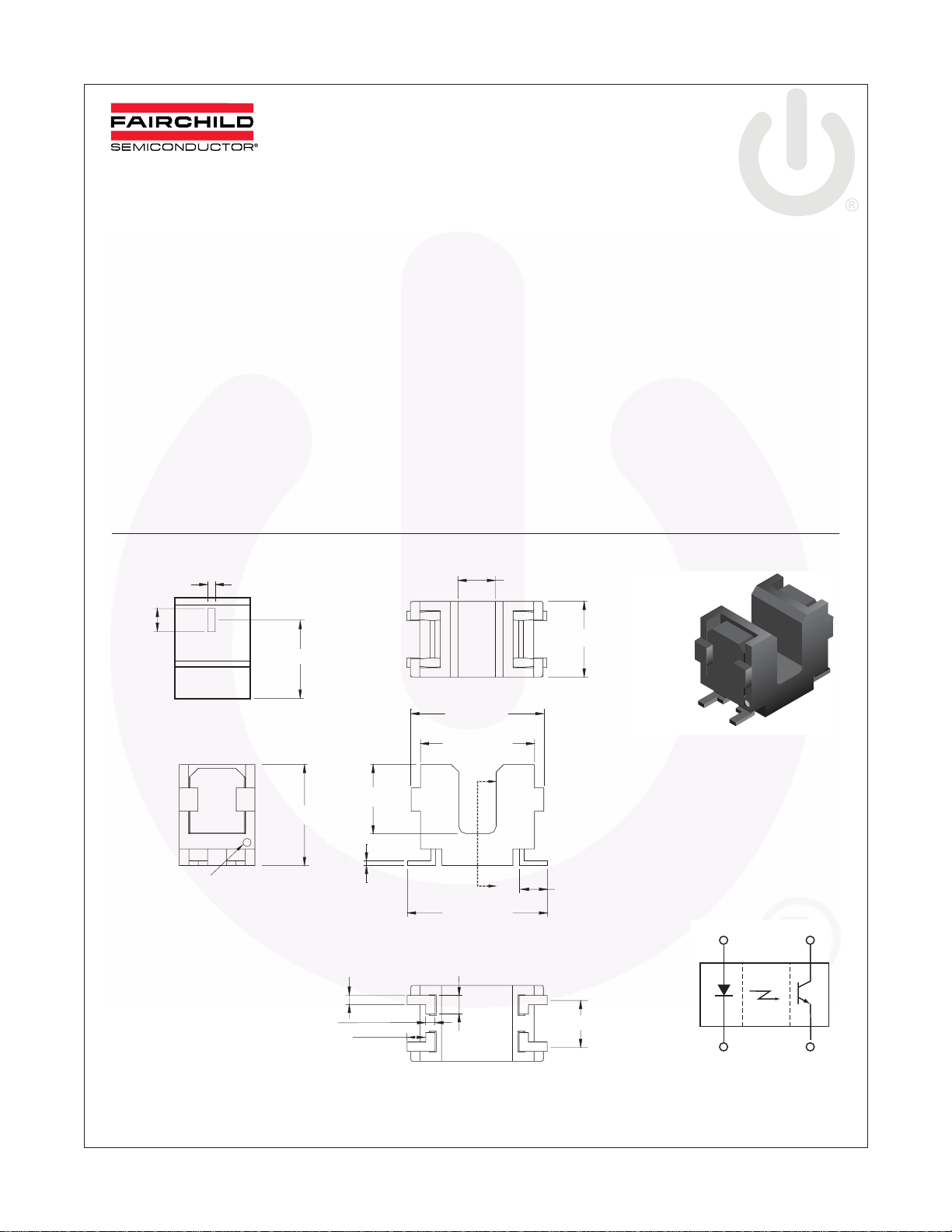
Package Dimension
0.016 (0.40)
0.049
(1.25)
0.165 (4.20)
SECTION "A-A"
Description
The QVE00033 is a miniature slotted optical switch
designed for surface mount applications. It consists of a
GaAs LED and a silicon phototransistor facing each
other across a 2mm gap, and packaged in a temperature
resistant black plastic housing.
0.079 (2.00)
0.159 (4.05)
0.276±0.01
(7.00±0.25)
0.240 (6.10)
"A"
0.146 (3.70)
0.213 (5.40)
DIMPLE
LEFT VIEW
0.020±0.002 (0.50±0.05) (4X)
0.039±0.002 (1.00±0.05) (4X)
Note:
1. Dimensions for all drawings are in inches (millimeters). Tolerance ±0.005" (0.127mm) unless othewise specified.
©2005 Fairchild Semiconductor Corporation www.fairchildsemi.com
QVE00033 Rev. 1.1.2
0.010±0.002
(0.25±0.05)
0.020±0.002
(0.50±0.05)
(4X)
(4X)
ANODE
CATHODE
"A"
0.295 (7.50)
0.039±0.002
(1.00±0.05)
BOTTOM VIEW
(4X)
0.059±0.008
(1.50±0.20)
COLLECTOR
0.099 (2.50)
EMITTER
1
2 3
4

QVE00033 — Phototransistor Optical Surface Mount Interrupter Switch
Absolute Maximum Ratings
(T
= 25°C unless otherwise specified)
A
Stresses exceeding the absolute maximum ratings may damage the device. The device may not function or be
operable above the recommended operating conditions and stressing the parts to these levels is not recommended.
In addition, extended exposure to stresses above the recommended operating conditions may affect device reliability.
The absolute maximum ratings are stress ratings only.
Symbol Parameter Rating Units
T
OPR
T
STG
T
SOL-I
T
SOL-F
P
TOT
EMITTER
I
F
V
R
P
D
SENSOR
V
CEO
V
ECO
I
C
P
D
Notes:
1. Derate power dissipation linearly 1.00mW/°C above 25°C.
2. RMA flux is recommended.
3. Methanol or isopropyl alcohols are recommended as cleaning agents.
4. Soldering iron tip 1/16" (1.6mm) from housing.
Operating Temperature -55 to +100 °C
Storage Temperature -55 to +100 °C
Soldering T emperature (Iron)
Soldering T emperature (Flow)
(2,3,4)
(2,3)
240 for 5 sec. °C
260 for 10 sec. °C
Total Power Dissipation 100 mW
Continuous Forward Current 50 mA
Reverse Voltage 6 V
Power Dissipation
(1)
75 mW
Collector-Emitter V oltage 30 V
Emitter-Collector V oltage 4.5 V
Collector Current 20 mA
Power Dissipation
(1)
75 mW
Electrical/Optical Characteristics
(T
= 25°C unless otherwise specified)
A
Symbol Parameter Test Conditions Min. Typ. Max. Units
EMITTER
V
l
I
PE
R
Forward Voltage
F
Reverse Current
Peak Emission Wavelength
SENSOR
I
CEO
Dark Current
COUPLED
I
C(ON)
V
CE (SAT)
t
t
©2005 Fairchild Semiconductor Corporation www.fairchildsemi.com
QVE00033 Rev. 1.1.2 2
Collector Current
Collector Emitter I
Rise Time
r
Fall Time 7 150 µs
f
I
= 20mA
F
V
= 4V
R
I
= 20mA
F
V
= 20V, I
CE
I
= 5mA, V
F
= 10mA, I
F
V
= 5V, R
CC
= 100µA
I
C
= 0mA
F
= 5V
CE
= 40µA
C
= 1000
L
1.2 1.4 V
10 µA
940 nm
100 nA
100 600 µA
0.4 V
Ω
,
7 150 µs
 Loading...