Fairchild QSE773 service manual

QSE773 — Sidelooker Pin Photodiode
August 2011
QSE773
Sidelooker Pin Photodiode
Features
■
Daylight filter
Sidelooker package
■
■
Pin photodiode
Wide reception angle, 120°
■
■
Chip size = 0.107 sq. inches (2.71 sq. mm)
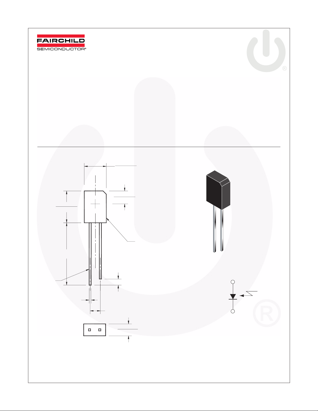
Package Dimensions
0.215 (5.46)
0.199 (5.06)
0.126 (3.20)
0.110 (2.80)
0.311 (7.90)
0.288 (7.30)
0.610 (15.49)
MIN
C
L
Description
The QSE773 is a plastic silicon pin photodiode in a
sidelooker package.
SENSING
SURFACE
Schematic
ANODE
0.020 (0.51)
SQ. (2x)
Notes:
1. Dimensions for all drawings are in inches (mm).
2. Tolerance of ±0.010 (0.25) on all non-nominal dimensions unless otherwise specified.
©2011 Fairchild Semiconductor Corporation www.fairchildsemi.com
FODMXXX Rev. 1.0.1
0.060 (1.52)
0.100 (2.54)
0.116 (2.95)
0.100 (2.54)
ANODE
CATHODE

Θ
(T
Absolute Maximum Ratings
= 25°C unless otherwise noted)
A
Stresses exceeding the absolute maximum ratings may damage the device. The device may not function or be
operable above the recommended operating conditions and stressing the parts to these levels is not recommended.
In addition, extended exposure to stresses above the recommended operating conditions may affect device reliability.
The absolute maximum ratings are stress ratings only.
Symbol Parameters Value Units
T
OPR
T
STG
T
SOL-I
T
SOL-F
V
P
Notes:
3. Derate power dissipation linearly 2.50mW/°C above 25°C.
4. RMA flux is recommended.
5. Methanol or Isopropyl alcohols are recommended as cleaning agents.
6. Soldering iron tip 1/16” (1.6 mm) from housing.
7. As long as leads are not under any stress or spring tension.
Operating Temperature -40 to +85 °C
Storage Temperature -40 to +85 °C
Soldering Temperature (Iron)
Soldering Temperature (Flow)
Reverse Voltage 32 V
R
Power Dissipation
D
(3)
150 mW
(4)(5)(6)(7)
(4)(5)(7)
240 for 5 sec. °C
260 for 10 sec °C
QSE773 — Sidelooker Pin Photodiode
Electrical Characteristics
(T
A
= 25°C)
Symbol Parameter Test Conditions Min. Typ. Max. Units
V
I
R(D)
λ
PK
I
PH
I
SC
C Capacitance V
t
t
Notes:
8. Light source is an GaAs LED which has a peak emission wavelength of 940nm.
9. All measurements made under pulse conditions.
Reverse Voltage I
R
Dark Reverse Current V
Peak Sensitivity V
= 0.1mA 32 V
R
= 10V 30 nA
R
= 5V 940 nm
R
Reception Angle at 1/2 Power ±60 °
Photo Current
Short Circuit Current
Rise Time V
r
Fall Time V
f
(8)
8)
E
= 1.0mW/cm
e
E
= 1.0mW/cm
e
= 3V 25 pF
R
= 5V, R
R
= 5V, R
R
= 1k Ω
L
= 1k Ω
L
2
, V
= 5V 30 µA
CE
2
18 µA
50 ns
50 ns
©2011 Fairchild Semiconductor Corporation www.fairchildsemi.com
FODMXXX Rev. 1.0.1 2
 Loading...