Fairchild QSE256, QSE257, QSE258, QSE259 service manual

tm
QSE256, QSE257, QSE258, QSE259 Plastic Silicon OPTOLOGIC® Photosensor
January 2011
QSE256, QSE257, QSE258, QSE259
Plastic Silicon OPTOLOGIC
®
Photosensor
Features
■
Bipolar silicon IC
Package type: Sidelooker
■
■
Medium wide reception angle, 50°
Package material and color: black epoxy
■
■
Daylight filter
High sensitivity
■
■
Direct TTL/LSTTL interface
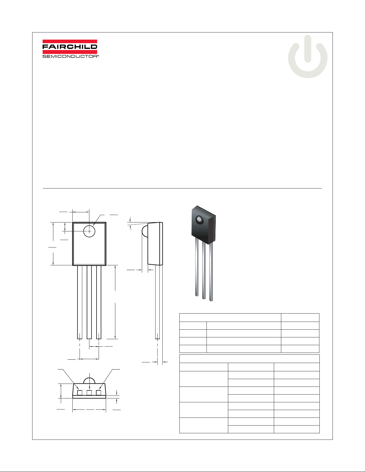
Package Dimensions
4.35
5.85
2.15
2.35
1.14
1.40
ø
1.39
1.65
0.67
0.77
Description
The QSE25x family are OPTOLOGIC® ICs which
feature a Schmitt trigger at output which provides hysteresis for noise immunity and pulse shaping. The basic
building block of this IC consists of a photodiode, a linear
amplifier, voltage regulator, Schmitt trigger and four output options. The TTL/LSTTL compatible output can drive
up to ten TTL loads over supply currents from 4.5 to 16.0
Volts. The devices are marked with a color stripe for
easy identification.
5° TYP ON ALL SIDES
12.7
MIN
Part Number Definitions Color Code
QSE256 Totem-Pole, buffer output Red
QSE257 Totem-Pole, inverter output Yellow
1.17
1.37
GND
1.45
1.71
2.34
2.74
Vout
4.38
4.62
Vcc
0.25
0.51
0.52
0.76
Note:
1. Dimensions for all drawings are in millimeters.
©2011 Fairchild Semiconductor Corporation www.fairchildsemi.com
QSE256, QSE257, QSE258, QSE259 Rev. 1.0.0
QSE258 Open-collector, buffer output Green
QSE259 Open-collector, inverter output Blue
Input/Output Table
Part Number Light Output
QSE256 On HIGH
Off LOW
QSE257 On LOW
Off HIGH
QSE258 On HIGH
Off LOW
QSE259 On LOW
Off HIGH

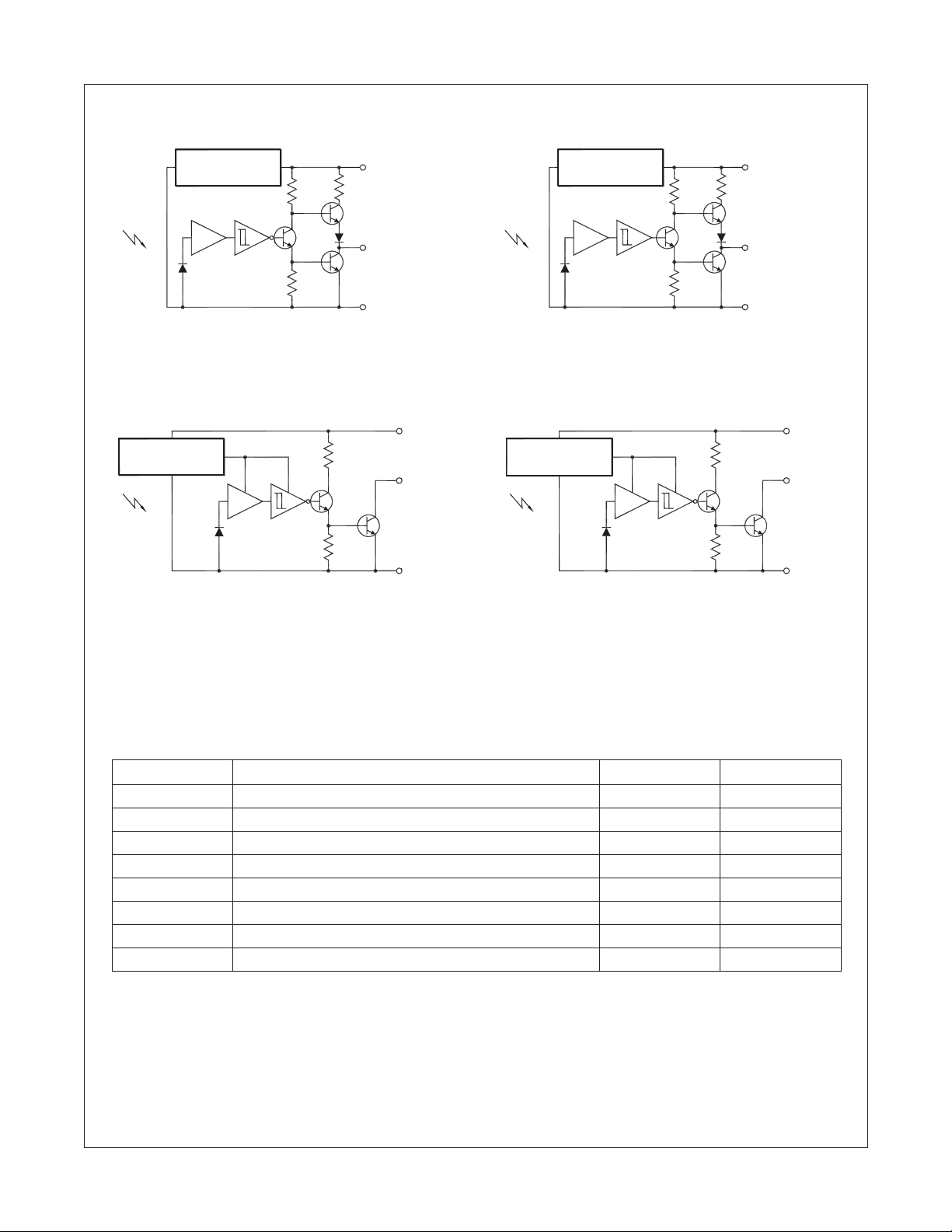
Block Diagrams
QSE256, QSE257, QSE258, QSE259 Plastic Silicon OPTOLOGIC® Photosensor
REGULATOR
LA
VOLTAGE
REGULATOR
Open-Collector Output Buffer
VOLTAGE
QSE256
Totem-Pole Outp
LA
QSE258
ut Buffer
V
CC
V
OUT
GND
V
CC
V
OUT
GND
VOLTAGE
REGULATOR
LA
V
CC
V
OUT
GND
QSE257
Totem-Pole Output Inverter
VOLTAGE
REGULATOR
LA
V
CC
V
OUT
GND
QSE259
Open-Collector Output Inverter
(T
Absolute Maximum Ratings
= 25°C unless otherwise specified)
A
Stresses exceeding the absolute maximum ratings may damage the device. The device may not function or be
operable above the recommended operating conditions and stressing the parts to these levels is not recommended.
In addition, extended exposure to stresses above the recommended operating conditions may affect device reliability.
The absolute maximum ratings are stress ratings only.
Symbol Parameter Rating Unit
T
OPR
T
STG
T
SOL-I
T
SOL-F
I
O
V
CC
V
O
P
D
Notes:
1. Derate power dissipation linearly 2.50mW/°C above 25°C.
2. RMA flux is recommended.
3. Methanol or isopropyl alcohols are recommended as cleaning agents.
4. Soldering iron tip 1/16" (1.6mm) minimum from housing.
Operating Temperature -40 to +85 °C
Storage Temperature -40 to +100 °C
Soldering Temperature (Iron)
Soldering Temperature (Flow)
(2,3,4)
(2,3)
240 for 5 sec °C
260 for 10 sec °C
Output Current 50 mA
Supply Voltage 4.0 to 16 V
Output Voltage 35 V
Power Dissipation
(1)
100 mW
©2011 Fairchild Semiconductor Corporation www.fairchildsemi.com
QSE256, QSE257, QSE258, QSE259 Rev. 1.0.0 2

5. λ
(T
Electrical Characteristics
= -40°C to +85°C, V
A
= 4.5V to 5.5V)
CC
Symbol Parameter Test Conditions Min. Typ. Max. Units
Ee(+) Positive Going Threshold
Irradiance
(5)
Ee(+)/Ee(-) Hysteresis Ratio 1.10 2.00
I
CC
Supply Current
(5)
Peak to Peak Ripple which
will Cause False Triggering
QSE256 (Buffer Totem Pole)
V
OH
V
OL
High Level Output Voltage
Low Level Output Voltage Ee = 0, I
QSE257 (Inverter Totem Pole)
V
OH
V
OL
High Level Output Voltage Ee = 0, I
Low Level Output Voltage
QSE258 (Buffer Open Collector)
I
OH
V
OL
High Level Output Current
Low Level Output Voltage Ee = 0, I
QSE259 (Inverter Open Collector)
I
OH
V
OL
High Level Output Current Ee = 0, V
Low Level Output Voltage
QSE256, QSE257
t
t
PHL
, t
R
, t
Output Rise, Fall Times Ee = 0 or 0.3mW/cm
F
Propagation Delay 6.0 µS
PLH
QSE258, QSE259
t
t
PHL
, t
R
, t
Output Rise, Fall Times Ee = 0 or 0.3mW/cm
F
Propagation Delay 6.0 µS
PLH
Note:
= 880nm (AlGaAs).
T
= 25°C 0.025 0.250 mW/cm
A
Ee = 0 or 0.3mW/cm
2
f = DC to 50MHz 2.00 V
(5)
Ee = 0.3mW/cm
OL
(5)
Ee = 0.3mW/cm
(5)
Ee = 0.3mW/cm
(5)
Ee = 0.3mW/cm
OH
OL
f = 10kHz, DC = 50%,
R
= 360 Ω
L
f = 10kHz, DC = 50%,
R
= 360 Ω
L
2
, I
= -10mA 2.4 V
OH
= 16mA 0.40 V
= -10mA 2.4 V
2
, I
= 16mA 0.40 V
OL
2
, V
= 30V 100 µA
OH
= 16mA 0.40 V
= 30V 100 µA
OH
2
, I
= 16mA 0.40 V
OL
2
,
(5)
2
,
(5)
5.0 mA
70 nS
100 nS
QSE256, QSE257, QSE258, QSE259 Plastic Silicon OPTOLOGIC® Photosensor
2
©2011 Fairchild Semiconductor Corporation www.fairchildsemi.com
QSE256, QSE257, QSE258, QSE259 Rev. 1.0.0 3
 Loading...