QRD1113, QRD1114 — Reflective Object Sensor
January 2008
QRD1113, QRD1114
Reflective Object Sensor
Features
■
Phototransistor Output
No contact surface sensing
■
■
Unfocused for sensing diffused surfaces
Compact Package
■
■
Daylight filter on sensor
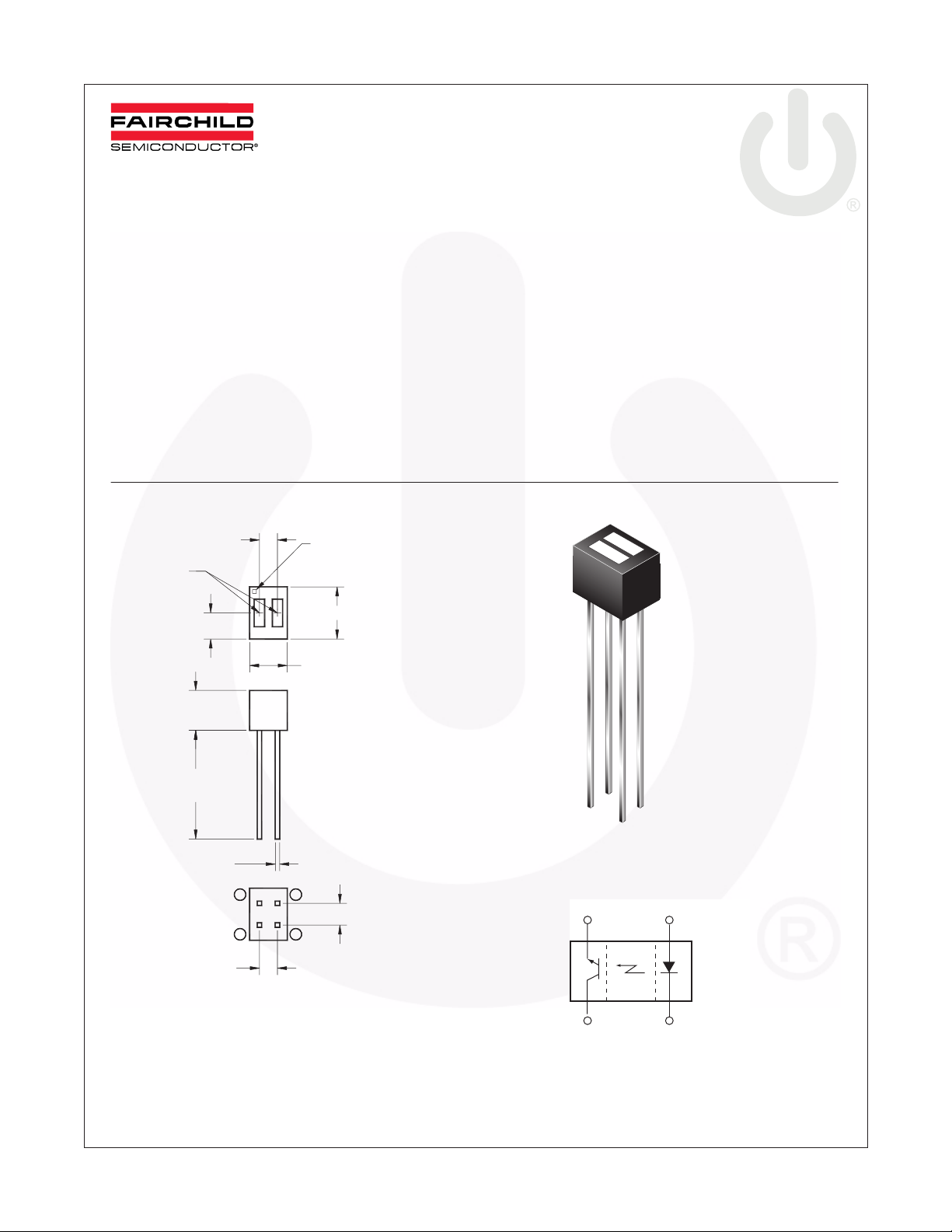
PACKAGE DIMENSIONS
Package Dimensions
0.083 (2.
OPTICAL
CENTERLI
NE
0.120 (3.
0.183 (4.
11)
05)
65)
PIN 1
0.240 (6.
0.173 (4.39)
Description
The QRD1113/14 reflective sensor consists of an infrared emitting diode and an NPN silicon phototransistor
mounted side by side in a black plastic housing. The onaxis radiation of the emitter and the on-axis response of
the detector are both perpendicular to the face of the
QRD1113/14. The phototransistor responds to radiation
emitted from the diode only when a reflective object or
surface is in the field of view of the detector.
INDICATOR
10)
0.500 (12.7)
MIN
0.020 (0.51)
SQ. (4X)
2
1
0.083 (2.
11)
PIN 1 COLLECTOR
PIN 2 EMITTER PIN 4 CATHODE
Notes:
1. Dimensions for all drawings are in inches (millimeters).
2. Tolerance of ± .010 (.25) on all non-nominal dimensions unless otherwise specified.
3. Pins 2 and 4 typically .050" shorter than pins 1 and 3.
4. Dimensions controlled at housing surface.
©2005 Fairchild Semiconductor Corporation www.fairchildsemi.com
QRD1113, QRD1114 Rev. 1.1.0
3
4
PIN 3
0.100 (2.
ANODE
54)
Schematic
23
14

QRD1113, QRD1114 — Reflective Object Sensor
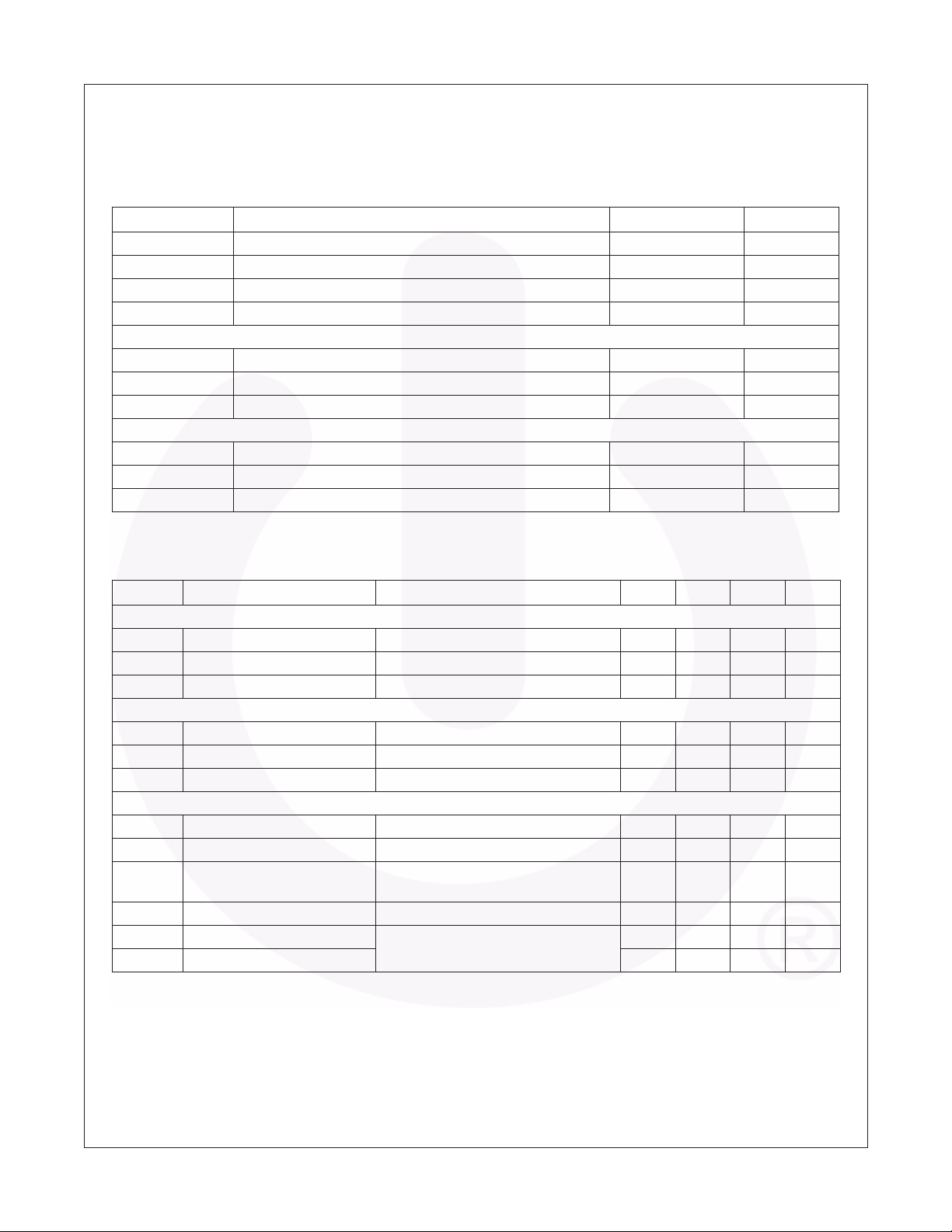
Absolute Maximum Ratings
(T
= 25°C unless otherwise specified)
A
Stresses exceeding the absolute maximum ratings may damage the device. The device may not function or be
operable above the recommended operating conditions and stressing the parts to these levels is not recommended.
In addition, extended exposure to stresses above the recommended operating conditions may affect device reliability.
The absolute maximum ratings are stress ratings only.
Symbol Parameter Rating Units
T
OPR
T
STG
T
SOL-I
T
SOL-F
EMITTER
I
F
V
R
P
D
SENSOR
V
CEO
V
ECO
P
D
Electrical/Optical Characteristics
Operating Temperature -40 to +85 °C
Storage Temperature -40 to +100 °C
Lead Temperature (Solder Iron)
Lead Temperature (Solder Flow)
(2,3)
(2,3)
240 for 5 sec °C
260 for 10 sec °C
Continuous Forward Current 50 mA
Reverse Voltage 5 V
Power Dissipation
(1)
100 mW
Collector-Emitter Voltage 30 V
Emitter-Collector Voltage V
Power Dissipation
(1)
(T
A
= 25°C)
100 mW
Symbol Parameter Test Conditions Min. Typ. Max. Units
INPUT (Emitter)
V
I
λ
OUTPUT (Sensor)
BV
BV
I
COUPLED
I
C(ON)
I
C(ON)
V
CE(SAT)
I
CX
Forward Voltage I
F
Reverse Leakage Current V
R
Peak Emission Wavelength I
PE
Collector-Emitter Breakdown I
CEO
Emitter-Collector Breakdown I
ECO
Dark Current V
D
QRD1113 Collector Current I
QRD1114 Collector Current I
Collector Emitter Saturation
= 20mA 1.7 V
F
= 5V 100 µA
R
= 20mA 940 nm
F
= 1mA 30 V
C
= 0.1mA 5 V
E
= 10 V, I
CE
= 20mA, V
F
= 20mA, V
F
I
= 40mA, I
F
= 0mA 100 nA
F
= 5V, D = .050"
CE
= 5V, D = .050"
CE
= 100µA, D = .050"
C
(6,8)
(6,8)
0.300 mA
1mA
(6,8)
Voltage
Cross Talk I
Rise Time V
t
r
t
Fall Time 50 µs
f
= 20mA, V
F
= 5V, R
CE
= 5V, E
CE
= 100 Ω , I
L
(7)
= 0
E
= 5mA 10 µs
C(ON)
.200 10 µA
0.4 V
Notes:
1. Derate power dissipation linearly 1.33mW/°C above 25°C.
2. RMA flux is recommended.
3. Methanol or isopropyl alcohols are recommended as cleaning agents.
4. Soldering iron tip 1/16” (1.6 mm) minimum from housing.
5. As long as leads are not under any stress or spring tension.
6. D is the distance from the sensor face to the reflective surface.
7. Crosstalk (I
8. Measured using Eastman Kodak neutral white test card with 90% diffused reflecting as a reflecting surface.
©2005 Fairchild Semiconductor Corporation www.fairchildsemi.com
QRD1113, QRD1114 Rev. 1.1.0 2
) is the collector current measured with the indicated current on the input diode and with no reflective surface.
CK

QRD1113, QRD1114 — Reflective Object Sensor
Typical Performance Curves
Fig. 1 Forward Voltage vs.
1.60 10.0
1.40
1.20
1.00
0.20
0.60
- FORWARD VOLTAGE (mV)I
F
V
0.40
0.20
Fig. 4 Normalized Collector Dark Current vs.
- COLLECTOR DARK CURRENT
D
Forward Current
0.1
10
10
10
1.0
10
10
10
1.0 10 100
IF - FORWARD CURRENT (mA) IF - FORWARD CURRENT (mA) TA - AMBIENT TEMPERATURE (˚C)
2
1
-1
-2
-3
-50 -25 25 50 75 1000
Temperature
VCE = 10 V
T
- AMBIENT TEMPERATURE (˚C)
A
Fig. 2 Normalized Collector Current vs.
1.00
0.10
0.01
- COLLECTOR CURRENT (mA)
C
I
.001
Forward Current
VCE = 5 V
D = .05"
0
10 20 30 40 50
1.0
.9
.8
.7
.6
.5
.4
.3
.2
.1
0
NORMALIZED - COLLECTOR CURRENT (mA)
Fig. 5 Normalized Collector Current vs.
050100 150 200 250 300 350 400 450 500
REFLECTIVE SURFACE DISTANCE (mils)
Fig. 3 Normalized Collector Current vs.
Temperature
1.0
0.8
0.6
0.4
0.2
- COLLECTOR CURRENT (mA)
C
I
0
-50 -25 25 50 750
IF = 10 mA
= 5 V
V
CE
Distance
IF = 20 mA
V
= 5 V
CE
©2005 Fairchild Semiconductor Corporation www.fairchildsemi.com
QRD1113, QRD1114 Rev. 1.1.0 3

TRADEMARKS
Thefollowing includes registered and unregistered trademarks and service marks, owned by Fairchild Semiconductor and/or its global
subsidiaries, and is not intended to be an exhaustive list of all such trademarks.
®
ACEx
Build it Now™
CorePLUS™
CROSSVOLT™
CTL™
Current Transfer Logic™
EcoSPARK
®
EZSWITCH™ *
™
®
Fairchild
Fairchild Semiconductor
FACT Quiet Series™
FACT
FAST
FastvCore™
FlashWriter
®
®
®
®
®*
*EZSWITCH™ and FlashWriter
FPS™
®
FRFET
Global Power Resource
SM
Green FPS™
Green FPS™ e-Series™
GTO™
i-Lo™
IntelliMAX™
ISOPLANAR™
MegaBuck™
MICROCOUPLER™
MicroFET™
MicroPak™
MillerDrive™
Motion-SPM™
OPTOLOGIC
OPTOPLANAR
®
®
are trademarks of System General Corporation, used under license by Fairchild Semiconductor.
®
®
PDP-SPM™
Power220
Power247
POWEREDGE
Power-SPM™
PowerTrench
Programmable Active Droop™
QFET
®
®
®
®
®
QS™
QT Optoelectronics™
Quiet Series™
RapidConfigure™
SMART START™
®
SPM
STEALTH™
SuperFET™
SuperSOT™-3
SuperSOT™-6
SuperSOT™-8
SyncFET™
®
The Power Franchise
TinyBoost™
TinyBuck™
TinyLogic
®
TINYOPTO™
TinyPower™
TinyPWM™
TinyWire™
µSerDes™
®
UHC
Ultra FRFET™
UniFET™
VCX™
QRD1113, QRD1114 — Reflective Object Sensor
®
DISCLAIMER
FAIRCHILD SEMICONDUCTOR RESERVES THE RIGHT TO MAKE CHANGES WITHOUT FURTHER NOTICE TO ANY PRODUCTS
HEREIN TO IMPROVE RELIABILITY, FUNCTION, OR DESIGN. FAIRCHILD DOES NOT ASSUME ANY LIABILITY ARISING OUT OF THE
APPLICATION OR USE OF ANY PRODUCT OR CIRCUIT DESCRIBED HEREIN; NEITHER DOES IT CONVEY ANY LICENSE UNDER ITS
PATENT RIGHTS, NOR THE RIGHTS OF OTHERS. THESE SPECIFICATIONS DO NOT EXPAND THE TERMS OF FAIRCHILD’S
WORLDWIDE TERMS AND CONDITIONS, SPECIFICALLY THE WARRANTY THEREIN, WHICH COVERS THESE PRODUCTS.
LIFE SUPPORT POLICY
FAIRCHILD’S PRODUCTS ARE NOT AUTHORIZED FOR USE AS CRITICAL COMPONENTS IN LIFE SUPPORT DEVICES OR
SYSTEMS WITHOUT THE EXPRESS WRITTEN APPROVAL OF FAIRCHILD SEMICONDUCTOR CORPORATION.
As used herein:
1. Life support devices or systems are devices or systems
which, (a) are intended for surgical implant into the body or
(b) support or sustain life, and (c) whose failure to perform
when properly used in accordance with instructions for use
2. A critical component in any component of a life support,
device, or system whose failure to perform can be
reasonably expected to cause the failure of the life support
device or system, or to affect its safety or effectiveness.
provided in the labeling, can be reasonably expected to
result in a significant injury of the user.
PRODUCT STATUS DEFINITIONS
Definition of Terms
Datasheet Identification Product Status Definition
Advance Information Form
ative or In Design
This datasheet contains the design specifications for product
development. Specifications may change in any manner without notice.
This datasheet contains preliminary data; supplementary data will be
Preliminary
First Production
published at a later date. Fairchild Semiconductor reserves the right to
make changes at any time without notice to improve design.
This datasheet contains final specifications. Fairchild Semiconductor
No Identification Needed Full Production
reserves the right to make changes at any time without notice to improve
the design.
This datasheet contains specifications on a product that has been
Obsolete Not In Production
discontinued by Fairchild Semiconductor. The datasheet is printed for
reference information only.
Rev. I32
©2005 Fairchild Semiconductor Corporation www.fairchildsemi.com
QRD1113, QRD1114 Rev. 1.1.0 4
 Loading...