Fairchild QEB363 service manual

tm
QEB363 Subminiature Plastic Infrared Emitting Diode
September 2006
QEB363
Subminiature Plastic Infrared Emitting Diode
Features
■
T-3/4 (2mm) Surface Mount Package
Tape & Reel Option (See Tape & Reel Specifications)
■
■
Lead Form Options: Gullwing, Yoke, Z-Bend
■
Narrow Emission Angle, 24°
Wavelength = 940nm, GaAs
■
■
Clear Water Lens
Matched Photosensor: QSB363
■
■
High Radiant Intensity
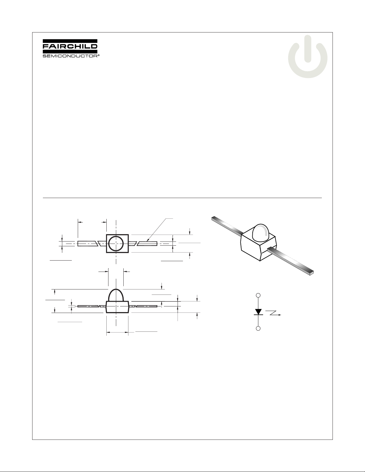
Package Dimensions
0.276 (7.0)
MIN
0.024 (0.6)
0.016 (0.4)
0.074 (1.9)
ANODE
0.087 (2.2)
0.071 (1.8)
0.019 (0.5)
0.012 (0.3)
Schematic
.118 (3.0)
.102 (2.6)
0.008 (0.21)
0.004 (0.11)
Notes:
1. Dimensions are in inches (mm).
2. Tolerance of ±.010 (.25) on all non nominal dimensions unless otherwise specified.
.059 (1.5)
.051 (1.3)
0.106 (2.7)
0.091 (2.3)
0.024 (0.6)
0.055 (1.4)
ANODE
©2002 Fairchild Semiconductor Corporation www.fairchildsemi.com
QEB363 Rev. 1.0.0

Θ
(T
Absolute Maximum Ratings
= 25°C unless otherwise specified)
A
Symbol Parameter Rating Unit
T
OPR
T
STG
T
SOL-I
T
SOL-F
I
F
V
R
P
D
Notes:
1. Derate power dissipation linearly 1.33mW/°C above 25°C.
2. RMA flux is recommended.
3. Methanol or isopropyl alcohols are recommended as cleaning agents.
4. Soldering iron 1/16" (1.6mm) minimum from housing.
Operating Temperature -40 to +100 °C
Storage Temperature -40 to +100 °C
Soldering Temperature (Iron)
Soldering Temperature (Flow)
(2,3,4)
(2,3)
240 for 5 sec °C
260 for 10 sec °C
Continuous Forward Current 50 mA
Reverse Voltage 5 V
Power Dissipation
(1)
100 mW
QEB363 Subminiature Plastic Infrared Emitting Diode
Electrical/Optical Characteristics
(T
A
= 25°C)
Symbol Parameter Test Conditions Min. Typ. Max. Units
λ
P
V
F
I
R
I
e
t
r
t
f
Peak Emission Wavelength I
Emission Angle I
Forward Voltage I
Reverse Current V
Radiant Intensity I
Rise Time I
Fall Time t
= 100mA 940 nm
F
= 100mA ±12 °
F
= 100mA, t
F
= 5V 100 µA
R
= 100mA, tp = 20ms 8 mW/sr
F
= 100mA 1 µs
F
= 20ms 1 µs
p
= 20ms 1.6 V
p
©2002 Fairchild Semiconductor Corporation www.fairchildsemi.com
QEB363 Rev. 1.0.0 2
 Loading...