Fairchild MPSA13, PZTA13, MPSA13, PZTA13 Schematics

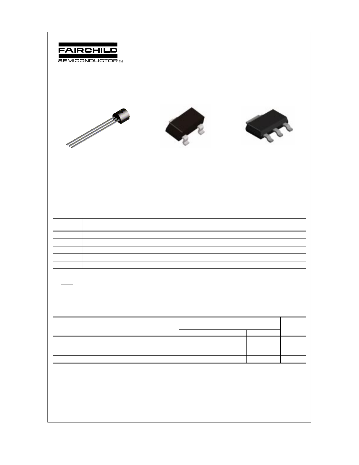
MMBTA13MPSA13 PZTA13
MPSA13 / MMBTA13 / PZTA13
C
E
C
B
E
TO-92
SOT-23
Mark: 1M
B
C
C
B
SOT-223
NPN Darlington Transistor
This device is designed for applications requiring extremely
high current gain at collector currents to 1.0 A. Sourced from
Process 05. See MPSA14 for characteristics.
Absolute Maximum Ratings* TA = 25°C unless otherwise noted
Symbol Parameter Value Units
V
CES
V
CBO
V
EBO
I
C
TJ, T
stg
*These ratings are limiting values above which the serviceability of any semiconductor device may be impaired.
NOTES:
1) These ratings are based on a maximum junction temperature of 150 degrees C.
2) These are steady state limits. The factory should be consulted on applications involving pulsed or low duty cycle operations.
Collector-Emitter Voltage 30 V
Collector-Base Voltage 30 V
Emitter-Base V ol tage 10 V
Collector Current - Continuous 1.2 A
Operating and Storage Junction Temperature Range -55 to +150
°C
E
Thermal Characteristics TA = 25°C unless otherwise noted
Symbol Characteristic Max Units
MPSA13 *MMBTA13 **PZTA13
P
D
R
θ
JC
R
θ
JA
*Device mounted on FR-4 PCB 1.6" X 1.6" X 0.06."
**Device mounted on FR-4 PCB 36 mm X 18 mm X 1.5 mm; mounting pad for the collector lead min. 6 cm
ã 1997 Fairchild Semiconductor Corporation
Total Device Dissipation
Derate above 25°C
Thermal Resistance, Junction to Case 83.3
Thermal Resistance, Junction to Ambient 200 357 125
625
5.0
350
2.8
2
1,000
8.0
.
mW
mW/°C
°C/W
°C/W

NPN Darlington Transistor
(continued)
Electrical Characteristics TA = 25°C unless otherwise noted
Symbol Parameter Test Conditions Min Max Units
OFF CHARACTERISTICS
V
(BR)CES
I
CBO
I
EBO
Collector-Emitter Breakdown
Voltage
Collector-Cutoff Current VCB = 30 V, IE = 0 100 nA
Em itte r-C uto ff C u rren t VEB = 10 V, IC = 0 100 nA
ON CHARACTERISTICS*
h
V
V
FE
CE(
BE(on)
sat
DC Current Gain IC = 10 mA, VCE = 5.0 V
Collector-Emitter Saturation Voltage IC = 100 mA, IB = 0.1 mA 1.5 V
)
Base-Emitter On V ol tage IC = 100 mA, VCE = 5.0 V 2.0 V
SMALL SIGNAL CHARACTERISTICS
f
T
Current Gain - Bandwi dth Product IC = 10 mA, VCE = 10 V,
*Pulse Test: Pulse Width £ 300 ms, Duty Cycle £ 2.0%
I
= 100 µA, IB = 0
C
= 100 mA, VCE = 5.0 V
I
C
f = 100 MHz
30 V
5,000
10,000
125 MHz
MPSA13 / MMBTA13 / PZTA13
 Loading...