AN-9036
Guidelines for Using Fairchild's Power56
Introduction
Dennis Lang, Staff Engineer
The Power56 minimizes both Printed Wiring Board (PWB) space and R
familiar SO-8 sized footprint, with the addition of a large drain tab for improving thermal
performance. The Power56 offers a footprint widely used in the industry for enhanced
performance SO-8 sized packages. This packaging technology requires mounting techniques,
which are slightly different from a conventional SO-8; however, those familiar with mounting
packages with large planar areas will find the techniques similar. This note will examine
techniques for mounting the Power56 in both prototype and manufacturing environments using
eutectic and lead free solder pastes.
in a convenient,
DS(ON)
Component Mounting
The process of attaching an electronic component to the PWB is the critical process in
determining performance and reliability of a MOSFET. Proper stencil and PWB design is
essential in getting the most out of a component, especially for a device utilizing an advanced
performance package like the Power56. Proper design of the process is also important for
reducing defects improving throughput and profitability of the assembly line. It has been
proposed that the “10x” rule applies to assembly defects. The implication is that as you progress
through the steps of the assembly, from printing solder to the end customer, the cost of a defect
rises tenfold per process step.
Board Layout
When designing a board for Power56, the designer should remember that the drain is the most
efficient at dissipating heat. Because of this there is the largest potential for gain by focusing on
1
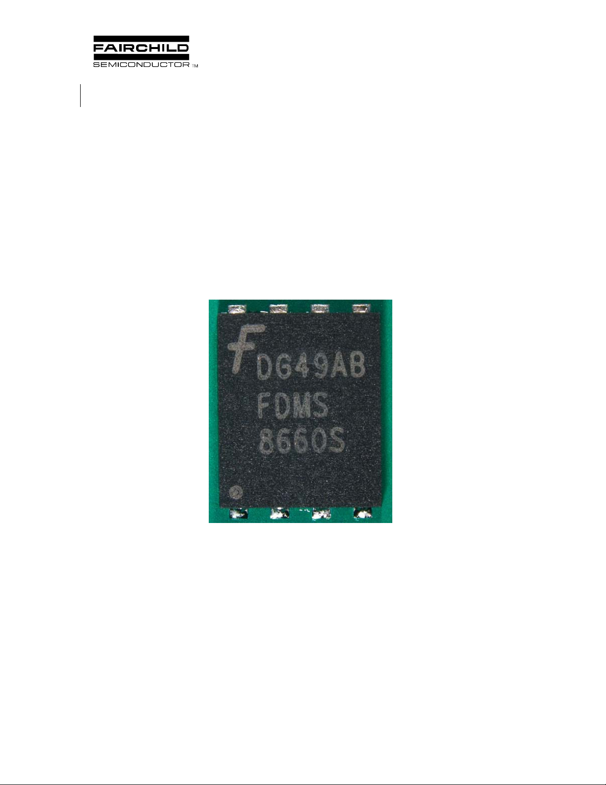
Figure 1: Power56 Mounted on PWB

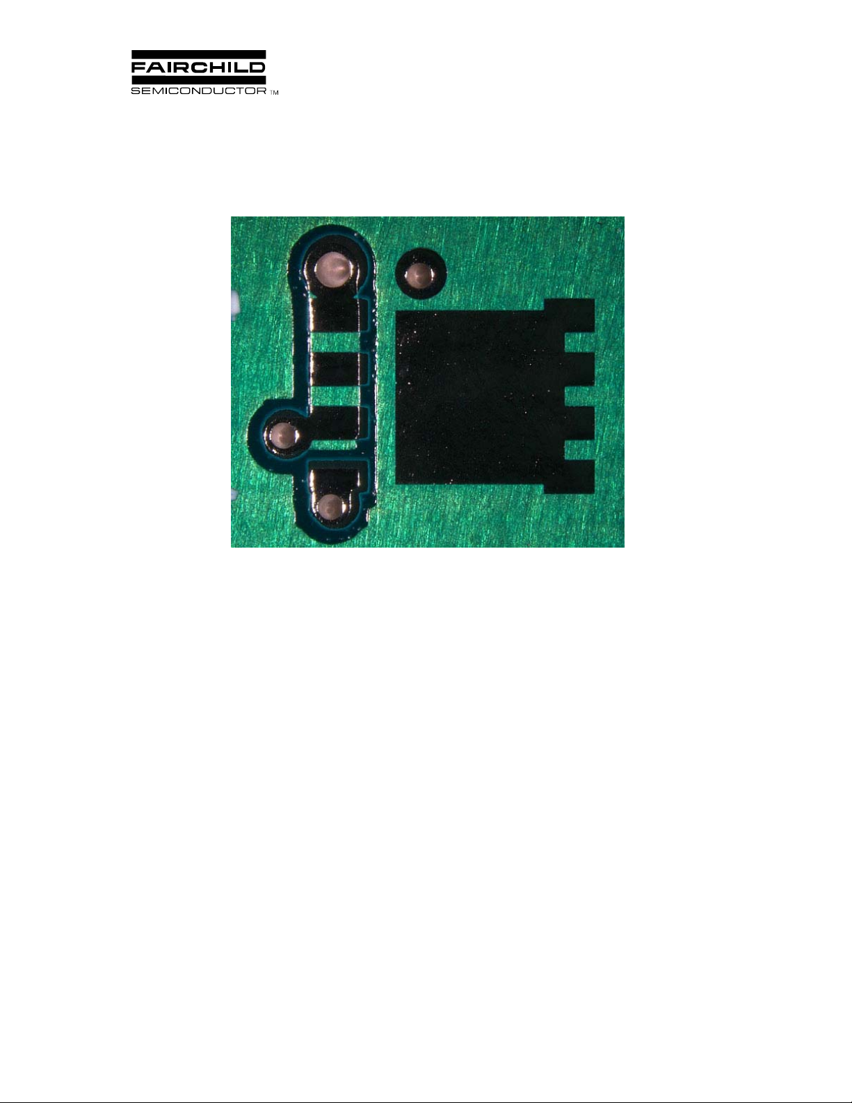
the drain heat sink and its heat path. Because of the unique design of the Power56 it is possible
to run copper traces from 3 sides of the die as seen below in figure 2. For best thermal
performance it is recommended that the user put as much copper on the drain as possible, while
keeping the thermal path short by keeping the area around the drain tab open. Pins 1-3 are
Source and pin 4 is the Gate. Pins 5-8 are part of the drain tab and make one continuous solder
joint with the drain tab. See the applicable data sheet for the specific pin out.
Figure 2: Power56 PWB footprint showing area around drain
lead allowing copper pour area for heat dissipation.
Via Usage with Power56
Note: This data was taken for the Fairchild FLMP package. It is applicable to the Power56 as
well. Customers frequently wish to use vias in their design to improve thermal performance by
using copper for heat dissipation on multiple layers of the PWB. Some papers suggest placing
vias in the drain pad for devices like TO-220. This is not recommended by the author. This
practice creates unpredictable solder joint formation as the wetting of solder into vias is random;
sometimes all of the vias will fill, sometimes none. Placing solder mask over the vias to keep
solder from wetting into the vias also creates voiding and is not recommended. It has been
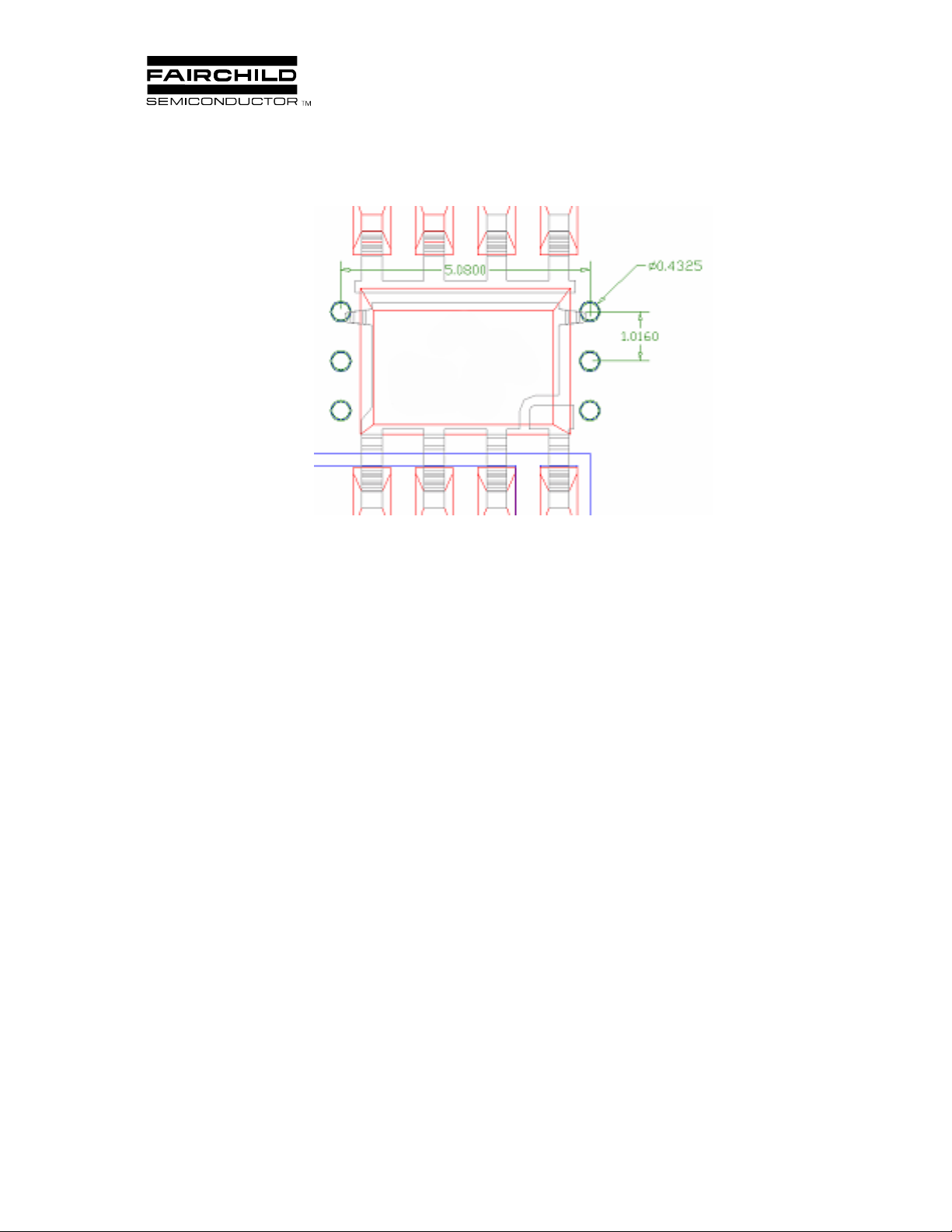
proven through Finite Element Analysis and supporting laboratory experimentation that placing
the vias just outside the pad will not cause an appreciable reduction in thermal performance, and
yield superior manufacturability. Figure 3 is a proven recommendation.
Solder Process
It has been estimated that 60% of all manufacturing defects are created at the solder deposition
phase. In modern surface mount electronics manufacturing, this means problems at stencil
printing. The design of the stencil is critical for the creation of a solder joint that exhibits superior
electrical and mechanical performance. As all designers involved in the design of stencils knows
there is not one design that will work for all applications. Differences in PWB finish, design,
solder paste and flux, reflow profile and dimensional accuracies for all of the related equipment
and machinery means ideally all stencils should be optimized for the specific application.
Because the stencil designer needs a “starting” point, it is recommended to focus on printing a
2

volume of solder paste that after reflow will be thick enough to cover the entire drain pad to a
thickness matching the maximum seating plane tolerance of the component. For the Fairchild
Power56, this tolerance is 0.06mm. A broad assumption used in the industry is that the volume
of solder paste will reduce by 50% due to reflow.
Figure 3: Recommended Via Size and Placement
Through testing in Fairchild’s SMT Apps Lab, it has been found that the stencil apertures
described below, and pictured in the appendix, are a good starting point, balancing adequate
solder volume to ensure a good joint, with concerns of excess solder volume and related defects
such as beading. Both stencil designs were found to be good places for the stencil designer to
start with. IPC-7525, Stencil Design Guidelines is also a good reference for all component types.
These stencil apertures were tested with Type 3 solder paste in eutectic tin lead and Lead Free
SAC 305 alloy compositions and found to deliver good performance with appropriate reflow
settings. (Though lead free paste is more “sticky” and as such care should be taken to verify the
process parameters such as rate of stencil separation and prints between cleaning if a stencil
originally designed for eutectic paste is used.) It is important to note that lead free paste solders
will not deliver wetting across the pad that process engineers have come to expect from eutectic
tin lead paste due to the high surface tension of tin present in high quantity in many lead free
alloys. The appearance of the solder joint itself is also frequently less shiny, even with good
process parameters.
Stencil Printing
The parameters used for printing in this study were, 5 mil thick electroformed stencil, 60º steel
squeegee, 1 psi squeegee pressure, and 25mm/s print speed. The solder paste vendor should
supply initial set-up information for your particular paste composition as speed and pressure is
paste dependant. The dimensioned stencil openings can be found in the appe ndix.
Solder Paste
Power56 components are normally used with one of the SAC tin/silver/copper lead free solder
paste alloys. IPC-9502, PWB Assembly Soldering Process Guideline for Electronic Components,
is a helpful reference for surface mount guidelines. Fairchild tests its components to 3 pass
reflow using a modified IPC/JEDEC J-STD-020B reflow profile, with the peak temp tested to
260ºC by Fairchild instead of the 250ºC of the standards committee. Further information on
Fairchild’s lead free effort can be found at:
http://www.fairchildsemi.com/products/lead_free/
3
 Loading...