PFCM Design Guide
PFCM Design Guide with Analog PFC IC
HP SPM & System Engineering Group
FAIRCHILD SEMICONDUCTOR
82-3, Dodang-Dong, Wonmi-ku, Puchon, Kyonggi-Do, KOREA
Tel) 82-32-680-1834, Fax) 82-32-680-1823
Feb. 2006 FAIRCHILD SEMICONDUCTOR – System Engineering Group
1

PFCM Design Guide
Contents
1. System Configurations.......................................................................... 3
2. Protection Circuits................................................................................. 3
Over Current Protection (OCP).............................................................................................................. 3
Over Voltage Protection......................................................................................................................... 4
Under Voltage Protection....................................................................................................................... 4
3. Design Example (PFCM DEMO BOARD).............................................. 5
Operating conditions of PFCM demo board:........................................................................................... 5
Output capacitance and Inductance design............................................................................................ 5
Output Voltage Ripple & Output Capacitance. .....................................................................................5
Inductance & Input Current Ripple ........................................................... ......... ..... .... ..... ......... ............ 6
Open Loop Response................................................................................................................................ 6
Current Loop Amplifier................................................... ....................................................................... 7
Voltage Loop Amplifier .......................................................................................................................... 7
Control Loop Implementation................................................................................................................ 8
Current Loop................................................. ....................................................... ................................... 8
Voltage Loop........................................................................................................................................... 9
Other Parameters................................ ....................................................... .......................................... 10
Over Current Protection....................................................................................................................... 12
Over Voltage Protection....................................................................................................................... 13
DC-link Voltage Control........................................................................................................................... 14
4. Experimental Results........................................................................... 15
Feb. 2006 FAIRCHILD SEMICONDUCTOR – System Engineering Group
2

1. System Configurations
PFCM Design Guide
V
ac
Relay
N/ F
V
TH
R
TH
S
R
NTC
Thermistor
P
R
SPM
IN
(S)
LVIC
IN
(R)
Shunt
Resistor
V
AC-
N
N
SENSE
Control IC
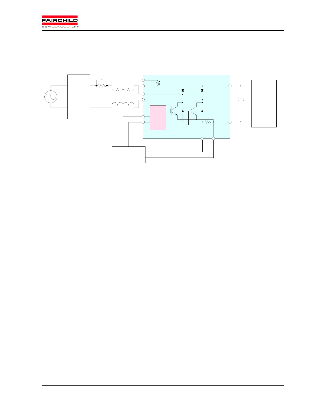
Fig.1 Typical block diagram of PFCM system
An inrush-current prevention circuit is required due to the large DC link capacitance as shown in Fig. 1.
The relay of the circuit should be closed after DC link capacitor is charged far enough. PFCM, mini-SPM and
control IC can share single GND stage. Usually, this GND and the N
terminal of PFCM should have the
SENSE
same potential. Large surge voltage is easily produced between P and N terminals by large current switching.
To reduce surge voltage it is important to shorten the DC link bus wiring between PFCM and DC link
capacitor. In addition, good high frequency characteristic capacitor, such as polypropylene film capacitor
should be mounted near to P and N terminals as a snubber.
2. Protection Circuits
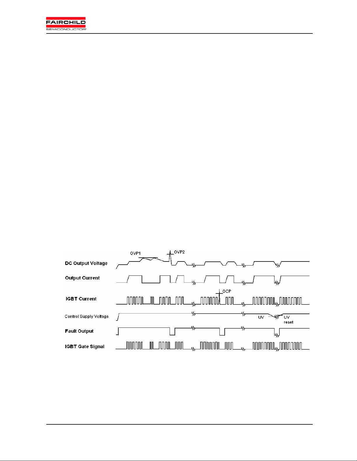
Following Fig. 2 shows the timing chart of protection function. There are two kind of protection level for
both OCP and OVP. Generally, PFC control ICs have its own OCP and OVP function. Also, user can make
the PFCM stop and output the FO signal under preset OC, OV condition using its Csc input.
Over Current Protection (OCP)
[OCP Level1 –P FCM ] PFCM can protect from over current situation. When OC(over current) situation
happens, the PFCM stops operating and generates fault out signal during fault-out duration time(set by C
And then after the duration, it works again according to the input command. Its total propagation delay time
may depend on outer op-amp speed. We recommend using a low cost slow op-amp solution with fast
protection. It is the OCP level2 protection described in next paragraph.
[OCP Level2 (SCP) –PFC control IC] By the peak current limit function of PFC control IC, the system
is protected from SC(Short Circuit) situation. The recommended current limit of OCP level 2 is higher than
FOD
).
Feb. 2006 FAIRCHILD SEMICONDUCTOR – System Engineering Group
3

PFCM Design Guide
that of OCP level 1. It doesn’t generate the fault out signal but its response is very fast. It will protect the
system from short circuit situation during the propagation delay time of OCP level1.
Over Voltage Protection
OV (Over Voltage) protection can be also implemented by dual protection. The DC-link voltage
changes slowly because of its large capacitance. So OVP does not need fast response. Therefore it is
optional to activate the OVP of PFC controller.
[OVP Level 1 - PFC co ntroller] OVP level 1 suppresses voltage overshoot in transient situation. It
doesn’t generate fault out signal.
[OVP Level 2 – PFCM] The voltage level of OVP level 2 is higher than that of OVP level 1. When OV
situation happens, the PFCM stops operating and generates fault out signal during fault-out duration time(set
by C
Under Voltage Protection
). And then it works again.
FOD
IGBT gate will be interrupted when control voltage drops below UV trip level, and the protection will be realeased
automatically if the control voltage recovers to the UV reset level.
Fig.2 Timing chart of protection function
Feb. 2006 FAIRCHILD SEMICONDUCTOR – System Engineering Group
4

PFCM Design Guide
3. Design Exa mple (PFCM DEMO BOARD)
A general PFC example is implemented for 5[kW] air-conditioning applications whose input voltage is
187~276[V].
Operating conditions of PFCM demo board:
Table 1. The operating conditions.
Item Symbol Value Unit
1 Switching Frequency Fsw 40 KHz
2 Minimum Input Voltage Vimin 176 Vac
3 Nominal Input Voltage Vinom 220 Vac
4 Maximum Input Voltage Vimax 264 Vac
5 Output Max. Power Po 5000 W
6 Minimum Output Voltage Vom in 350 Vdc
7 Nominal Output Voltage Vonom 380 Vdc
8 OVP level 1 V
9 OVP level 2 V
420 V
OV1
440 V
OV2
10 Peak Ripple Current Iripple 5 A
11 OCP Level1 Iocp1 40 A
12 OCP Level2 (SCP) Iocp2 50 A
13 Shunt Resistor Rsh 2 MOhm
14 DC Capacitor Cout 940 uF
Output capacitance and Inductance design
Output Voltage Ripple & Output Capacitance
Voltage ripple of V
(470[uF] x 2)
Feb. 2006 FAIRCHILD SEMICONDUCTOR – System Engineering Group
can be reduced by employing large C
DC
5
. In demo board, C
OUT
is set to 940[uF]
OUT

Inductance & Input Current Ripple
∴
where: ΔI
V
V
: Peak to peak current of PFC inductor
Lp-p
: Input AC voltage
IN
: DC link Voltage
OUTDC
f : Switching frequency
L : Inductance of PFC inductor
VVV
OUTDC
fL
4
INOUTDCIN
(
=Δ
I
L
PP
−
I
fLV
OUTDC
)( =Δ
PP
−
V
MAXL
PFCM Design Guide
)( −
1
VV
=∵
2
)
OUTDCIN
V
OUTDC
L
Î
AI
5)( =Δ
MAXL
PP
−
20Hf
380
==
4000020
⋅
=
][475
μ
(fs=40kHz)
Current ripple is decided by switching frequency and inductance. To reduce current ripple, high
switching frequency and large inductance value is required. It means that employing higher switching
frequency can reduce inductor size. But the power losses will increase and it requires more efficient heat
sink structure.
Open Loop Response
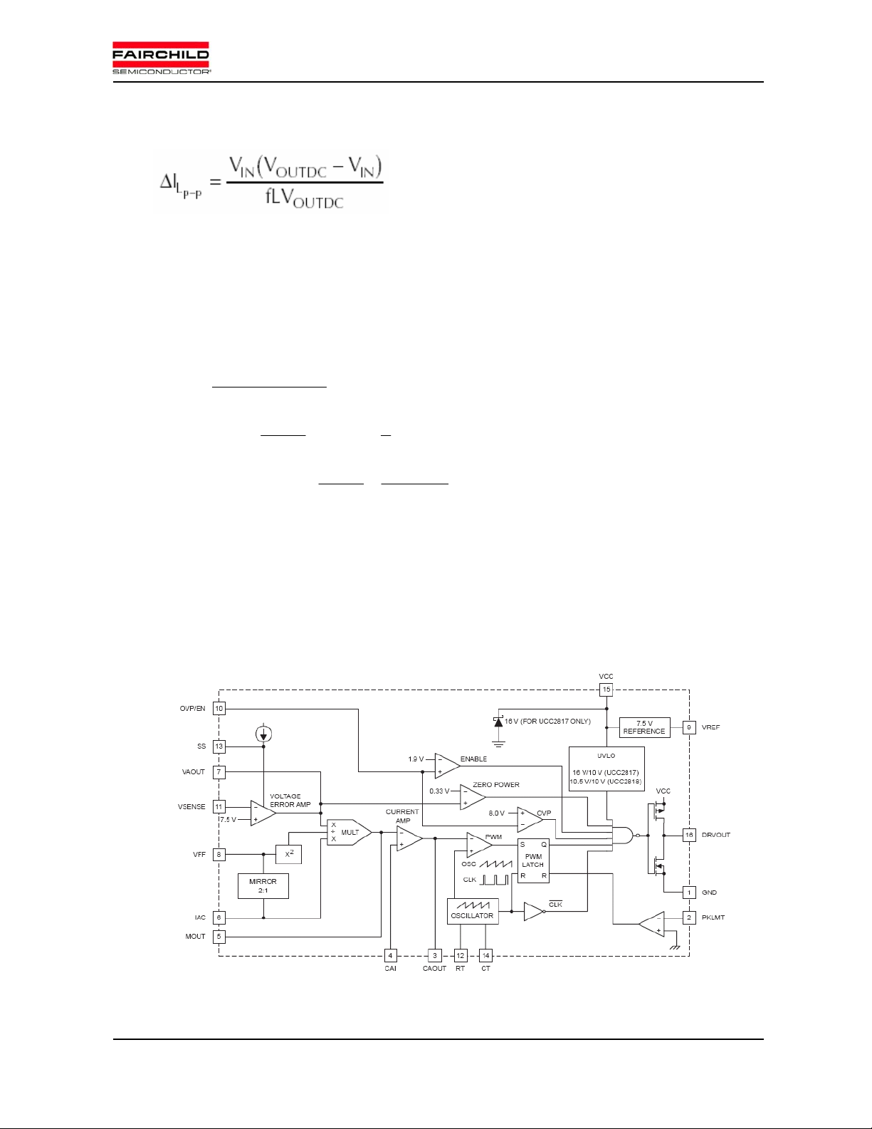
Fig.3 Block diagram of PFC control IC
Feb. 2006 FAIRCHILD SEMICONDUCTOR – System Engineering Group
6
 Loading...