

Page 1
Is Now Part of
To learn more about ON Semiconductor, please visit our website at
ON Semi conductor an d the ON Semico nductor logo a re trademar ks of Semicon ductor Comp onents Indus tries, L LC dba ON Semico nductor or it s subsidiari es in the United S tates and /or other coun tries. ON Se miconducto r owns the righ ts to a number
of patents, trademarks, copyrights, trade secrets, and other intellectual property. A listing of ON Semiconductor’s product/patent coverage may be accessed at www.onsemi.com/site/pdf/Patent-Marking.pdf. ON Semiconductor reserve s the right
to make changes without f urther noti ce to any produc ts herein. ON S emicon ductor makes no warran ty, representat ion or guar antee regar ding the suitability of its pro ducts for any partic ular purpose, n or does ON Semic onductor as sume any liabilit y
arisin g out of the applica tion or us e of any product o r circui t, and specific ally dis claims any and all lia bilit y, includin g witho ut limit ation sp ecial, c onsequential or incidental da mages . Buye r is responsib le for it s products and a pplica tions us ing ON
Semic onductor pr oducts, inc luding complia nce with all law s, regulati ons and safet y requirem ents or stan dards, rega rdless of an y support or ap plications in formation p rovided by ON S emiconduc tor. “Typical ” parameter s which may be pr ovided in ON
Semic onductor data s heet s and/or s pecificatio ns can and do vary in diff erent a pplica tions an d actual perf ormance may var y over time. All o perat ing parameter s, including “Typical s” must b e validated for e ach cus tomer ap plicat ion by customer’s
techni cal exper ts. ON Semic onductor do es not conve y any license un der its pate nt rights no r the rights o f others. ON S emiconduc tor produc ts are not des igned, inte nded, or autho rized for use a s a critical c omponent in lif e support s ystems or an y FDA
Clas s 3 medical devi ces or medica l devices wit h a same or similar c lassificat ion in a foreign j urisdictio n or any device s intended for im plantation in t he human body. Sho uld Buyer pur chase or use ON S emiconduct or products f or any such unint ended
or unaut horized appli cation, Buy er shall indemn ify and hold O N Semiconduc tor and its of ficers, e mployees , subsidiari es, affilia tes, and dis tributor s harmless ag ainst all claim s, costs , damages, an d expenses , and reason able attorn ey fees aris ing out
of, dire ctly or indire ctly, any claim o f personal inj ury or death as sociated w ith such unint ended or unauth orized use, e ven if such claim a lleges that ON S emiconduc tor was neglig ent regardin g the design or ma nufacture o f the part. ON S emiconduct or
is an Equa l Oppor tunity/Affirm ative Action E mployer. This li terature is s ubject to all applicable c opyright la ws and is no t for resale in any manner.
www.onsemi.com
Page 2
www.fairchildsemi.com
FSA642 — Evaluation Board User Guide
1. Introduction
This user guide is for the FSA642 evaluation board and is intended to complement the FSA642
datasheet. Technical or application-specific questions not addressed in this guide should be
directed to Fairchild’s technical support team. Please contact your Fairchild representative, visit
our website at www.fairchildsemi.com
This evaluation board is used to evaluate the high-speed performance of Fairchild’s differential
3PDT MIPI switch. SMA connectors are used for maintaining signal integrity of input and output
signals. The board is designed to pass differential clock or data signals without the use of onboard loads or terminations. Clock and data trace pairs are designed for 100Ω differential
impedance. For lab evaluation, a standard 50Ω pulse/data generator can supply signals into the
inputs and 50Ω terminated, high-bandwidth oscilloscope sampling heads can be used to
terminate the outputs.
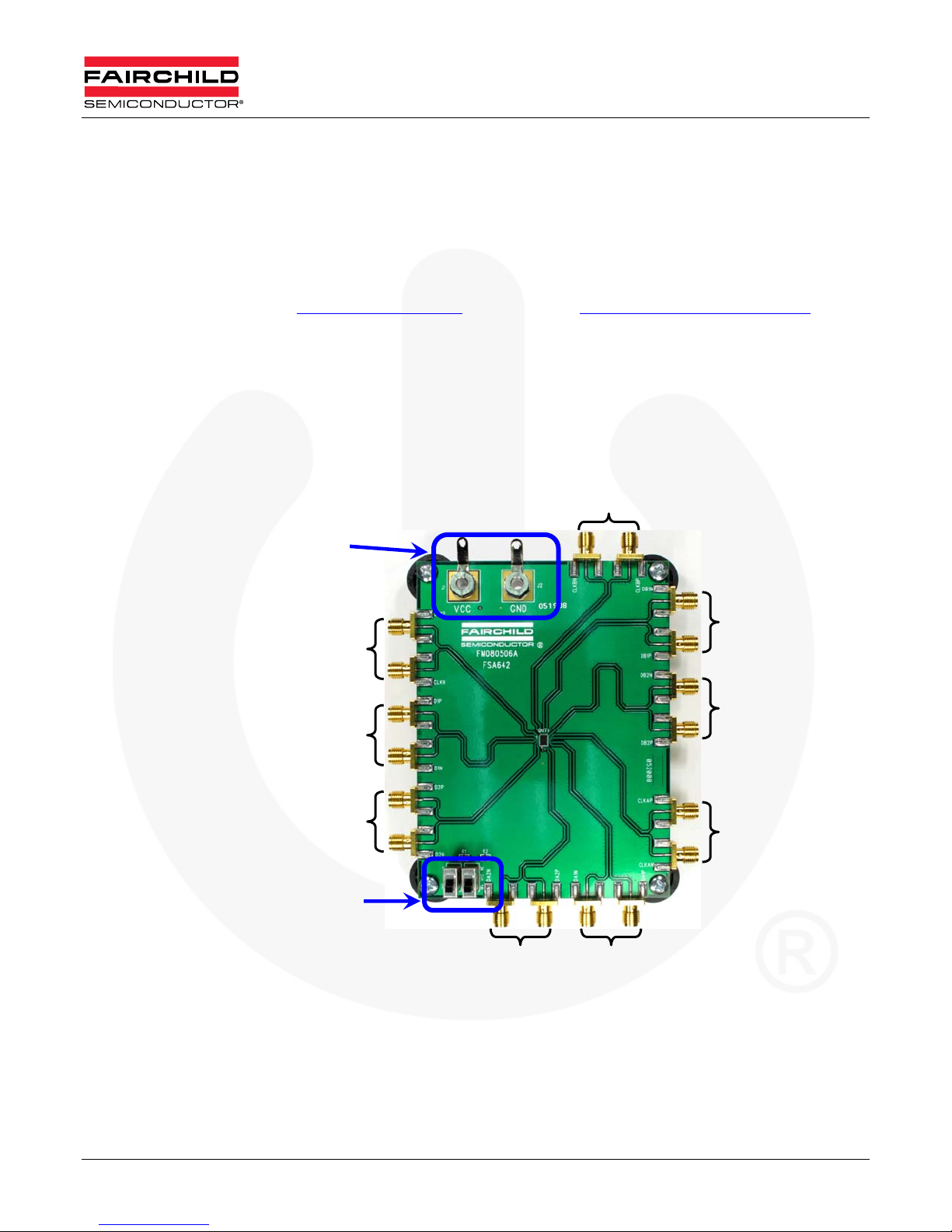
Power Supply
Connectors
, or contact us at analogswitch@fairchildsemi.com.
CLKB
D1B
CLK
D2B
D1
D2
CLKA
Control Switches
(SW1, SW2)
D2A
D1A
Figure 1. Evaluation Board with Component Locations Labeled
Configuration of the device is simplified by on-board switches to enable/disable the device and
to control the output select manually. Signal trace layout follows the UMLP package pad layout,
with clock/data inputs at the left and multiplexed outputs at top, right and bottom.
© 2009 Fairchild Semiconductor Corporation 1 FSA642 FEB • Rev. 0.0.1
Page 3

www.fairchildsemi.com
2. Getting Started
To begin using this evaluation board, perform the following steps:
1. Configure the on-board control pin switches in the desired state (see Table 1).
2. Connect signal cables or 50-Ω terminated scope cables to SMA connectors.
3. Apply power to the board at the power supply connectors.
Note: Per the datasheet, the recommended V
operation range is 2.65V to 4.3V.
CC
4. Enable input signals.
3. Control Pin Configuration
This FSA642 evaluation board has two mechanical SPDT switches located at the bottom left
corner. These configure the output enable (/OE) and output switch selection (SEL) functions of
the FSA642. Table 1 lists the position of the mechanical switches and the corresponding
functional states for the control inputs.
Table 1. Control Pin Configurations
SW1
(/OE)
SW2
(SEL)
n/a
Inputs disconnected from outputs
CLK, D1, D2 differential pairs connected to CLKA, D1A, D2A
FSA642 Switch Function
© 2009 Fairchild Semiconductor Corporation 2 FSA642 FEB • Rev. 0.0.1
CLK, D1, D2 differential pairs connected to CLKB, D1B, D2B
Page 4

www.fairchildsemi.com
© 2009 Fairchild Semiconductor Corporation 3 FSA642 FEB • Rev. 0.0.1
Figure 1. Application Board Schematic
Page 5

www.fairchildsemi.com
WARNING AND DISCLAIMER
Replace components on the Evaluation Board only with those parts shown on the parts list (or Bill of Materials) in the Users’ Guide. Contact an authorized Fairchild
representative with any questions.
The Evaluation board (or kit) is for demonstrati on purposes only and neither the Board nor this User’s Guide constitute a sales contract or create any kind of
warranty, whether express or implied, as to the applications or products involved. Fairchild warrantees that its products meet Fairchild’s publ ished speci ficati ons, but
does not guarantee that its products work in any specific application. Fairchild reserves the right to make changes without notic e to any products described herein to
improve reliability, function, or design. Either the applicable sales contract signed by Fairchild and Buyer or, if no contract exists, Fairchild’s standard Terms and
Conditions on the back of Fairchild invoices, govern the terms of sale of the products described herein.
DISCLAIMER
FAIRCHILD SEMICONDUCTOR RESERVES THE RIGHT TO MAKE CHANGES WITHOUT FURTHER NOTICE TO ANY PRODUCTS HEREIN TO IMPROVE
RELIABILITY, FUNCTION, OR DESIGN. FAIRCHILD DOES NOT ASSUME ANY LIABILITY ARISING OUT OF THE APPLICATION OR USE OF ANY PRODUCT
OR CIRCUIT DESCRIBED HEREIN; NEITHER DOES IT CONVEY ANY LICENSE UNDER ITS PATENT RIGHTS, NOR THE RIGHTS OF OTHERS.
LIFE SUPPORT POLICY
FAIRCHILD’S PRODUCTS ARE NOT AUTHORIZED FOR USE AS CRITICAL COMPONENTS IN LIFE SUPPORT DEVICES OR SYSTEMS WITHOUT THE
EXPRESS WRITTEN APPROVAL OF THE PRESIDENT OF FAIRCHILD SEMICONDUCTOR CORPORATION.
As used herein:
1. Life support devices or systems are devices or systems which, (a) are
intended for surgical implant into the body, or (b) support or sustain life, or
(c) whose failure to perform when properly used in accordance with
instructions for use provided in the labeling, can be reasonably expected to
result in significant injury to the user.
ANTI-COUNTERFEITING POLICY
Fairchild Semiconductor Corporation's Anti-Counterfeiting P olic y. Fairchild's Anti-Counterfeiti ng Pol icy is also stated on our external website, www.fairchildsemi.com,
under Sales Support.
Counterfeiting of semiconductor parts is a growing problem in the i ndustry. All manufacturers of semiconductor products are experiencing counterfeiting of their
parts. Customers who inadvertently purchase counterfeit parts experience many problems such as loss of brand reputation, substandard performance, failed
applications, and increased cost of production and manufacturing delays. Fairchild is taking strong measures to protect oursel ves and our customers from the
proliferation of counterfeit parts. Fairchild strongly encourages customers to purchase Fairchild parts either directly from Fairchild or from Authorized Fairchild
Distributors who are listed by country on our web page cited above. Products customers buy either from Fairchild directly or from Authorized Fairchild Distributors are
genuine parts, have full traceability, meet Fairchild's quality standards for handling and storage and provide access to Fairchild's full range of up-to-date technical
and product information. Fairchild and our Authorized Distributors will stand behind all warranties and will appropriately address any warranty issues that may arise.
Fairchild will not provide any warranty coverage or other assistance for parts bought from Unauthorized Sources. Fairchild is com mitted to combat this global
problem and encourage our customers to do their part in stopping this practice by buying direct or from authorized distributors.
2. A critical component is any component of a life support device or system
whose failure to perform can be reasonably expected to cause the failure of
the life support device or system, or to affect its safety or effectiveness.
Revision History
Date Reason for Change Revision #
04/02/10 Initial Draft (S.Barden) A0.0
© 2009 Fairchild Semiconductor Corporation 4 FSA642 FEB • Rev. 0.0.1
Page 6

ON Semiconductor and are trademarks of Semiconductor Components Industries, LLC dba ON Semiconductor or its subsidiaries in the United States and/or other countries.
ON Semiconductor owns the rights to a number of patents, trademarks, copyrights, trade secrets, and other intellectual property. A listing of ON Semiconductor’s product/patent
coverage may be accessed at www.onsemi.com/site/pdf/Patent−Marking.pdf
ON Semiconductor makes no warranty, representation or guarantee regarding the suitability of its products for any particular purpose, nor does ON Semiconductor assume any liability
arising out of the application or use of any product or circuit, and specifically disclaims any and all liability, including without limitation special, consequential or incidental damages.
Buyer is responsible for its products and applications using ON Semiconductor products, including compliance with all laws, regulations and safety requirements or standards,
regardless of any support or applications information provided by ON Semiconductor. “Typical” parameters which may be provided in ON Semiconductor data sheets and/or
specifications can and do vary in different applications and actual performance may vary over time. All operating parameters, including “Typicals” must be validated for each customer
application by customer’s technical experts. ON Semiconductor does not convey any license under its patent rights nor the rights of others. ON Semiconductor products are not
designed, intended, or authorized for use as a critical component in life support systems or any FDA Class 3 medical devices or medical devices with a same or similar classification
in a foreign jurisdiction or any devices intended for implantation in the human body. Should Buyer purchase or use ON Semiconductor products for any such unintended or unauthorized
application, Buyer shall indemnify and hold ON Semiconductor and its officers, employees, subsidiaries, affiliates, and distributors harmless against all claims, costs, damages, and
expenses, and reasonable attorney fees arising out of, directly or indirectly, any claim of personal injury or death associated with such unintended or unauthorized use, even if such
claim alleges that ON Semiconductor was negligent regarding the design or manufacture of the part. ON Semiconductor is an Equal Opportunity/Affirmative Action Employer. This
literature is subject to all applicable copyright laws and is not for resale in any manner.
PUBLICATION ORDERING INFORMATION
LITERATURE FULFILLMENT:
Literature Distribution Center for ON Semiconductor
19521 E. 32nd Pkwy, Aurora, Colorado 80011 USA
Phone: 303−675−2175 or 800−344−3860 Toll Free USA/Canada
Fax: 303−675−2176 or 800−344−3867 Toll Free USA/Canada
Email: orderlit@onsemi.com
© Semiconductor Components Industries, LLC
. ON Semiconductor reserves the right to make changes without further notice to any products herein.
N. American Technical Support: 800−282−9855 Toll Free
USA/Canada
Europe, Middle East and Africa Technical Support:
Phone: 421 33 790 2910
Japan Customer Focus Center
Phone: 81−3−5817−1050
ON Semiconductor Website: www.onsemi.com
Order Literature: http://www.onsemi.com/orderlit
For additional information, please contact your local
Sales Representative
www.onsemi.com
1
www.onsemi.com
 Loading...