

Page 1
NC7SB3257
NC7SB3257 TinyLogic
January 2000
Revised April 2002
TinyLogic
UHS
2:1 Multiplexer/Demultiplexer Bus Switch
General Description
The NC7SB3257 is a high performance, 2:1 NM OS passgate multiplexer/demultiplexer from Fairchild’s Ultra High
Speed Series of TinyLogic
advanced sub-micron CMOS technology to achieve high
speed enable and disable time s and low On Resistance.
The device is specified to operate over the 4.0 to 5.5V V
operating range. T he control input to lerates volt ages up to
5.5V independent of the V
. The device is fabricated with
operating range.
CC
Ordering Code:
Order
Number
NC7SB3257P6X MAA06A B7B 6-Lead SC70, EIAJ SC88, 1.25mm Wide 3k Units on Tape and Reel
NC7SB3257L6X MAC06A B7 6-Lead MicroPak, 1.0mm Wide 5k Units on Tape and Reel
Package
Number
Product Code
Top Mark
Features
■ Space saving SC70 6-lead surface mount package
■ Ultra small MicroPak
■ Typical 3
■ Minimal propagation delay through the switch
■ Power down high impedance cont rol input
CC
■ Zero bounce in flow through mode
■ TTL compatible control input
■ Overvoltage tolerance of control input to 7.0V
■ Break before make enable circuitry
Package Descript ion Supplied As
Ω switch resistance @ 5.0V V
leadless package
CC
UHS 2:1 Multiplexer/Demultiplexer Bus Switch
TinyLogic and MicroPa k are trademarks of Fairchild Semico nductor Corporatio n.
© 2002 Fairchild Semiconductor Corporation DS500325 www.fairchildsemi.com
Page 2
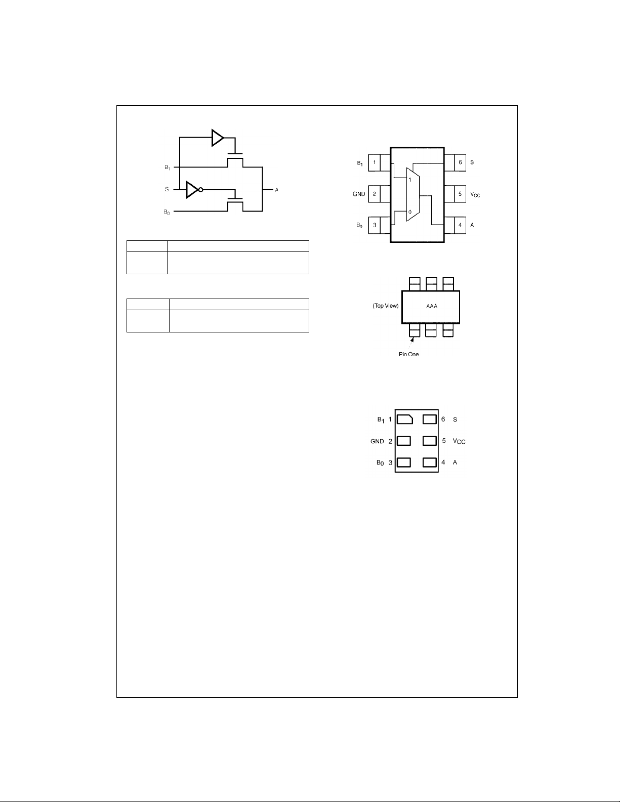
Logic Symbol
NC7SB3257
Pin Descriptions
Pin Names Description
, B
A, B
0
1
S Control Input
Function Table
Input (S) Function
LB
HB
H = HIGH Logic Level
L = LOW Logic Level
Data Ports
Connected to A
0
Connected to A
1
Connection Diagrams
Pin Assignments for SC70
(Top View)
Pin One Orientation Diagram
AAA = Product Code Top Mark - see ordering code
Note: Orientation of Top Mark determines Pin One location. Read the top
product code mark lef t to right, Pin One is the lo w er left pin (see diagram ).
Pad Assignments for MicroPak
www.fairchildsemi.com 2
(Top Thru View)
Page 3
Absolute Maximum Ratings(Note 1) Recommended Operating
Supply Voltage (VCC) −0.5V to +7.0V
DC Switch Voltage (V
DC Output Voltage (V
DC Input Diode Current (I
@ (I
) VIN < 0V −50 mA
IK
DC Output Current (I
or Ground Current (ICC/I
DC V
CC
Storage Temperature Range (T
Junction Lead Temperature under Bias (T
Lead Temperature (T
(Soldering, 10 seconds)
Power Dissipation (P
) −0.5V to +7.0V
S
) −0.5V to +7.0V
IN
)
IK
) 128 mA
OUT
L
)
) ±100 mA
GND
) −65°C to +150°C
STG
) +150°C
J
+260°C
) @ +85°C180 mW
D
Conditions
Supply Voltage Operating (V
Control Input Voltage (V
Switch Input Voltage (VIN)0V to V
Output Voltage (V
Operating Temperature (TA) −40°C to +85°C
Input Rise and Fall Time (t
Control Input V
Thermal Resistance (
Note 1: Absolute maximum ratings are DC values beyond which t he devi ce
may be damag ed or hav e it s usefu l li fe i mpa ired. Th e da tas heet sp ecific ations should be met, without exception, to ensure that the system design is
reliable over its power supply, temperature, and output/input loading variables. Fairchild does not recommend operation outside datasheet specifications.
Note 2: Control input mu s t be held HIGH or LOW, it must not float .
Note 3: The input and output negative voltage ratings may be exceeded if
the input and ou t put diode curr ent ratings ar e observed.
(Note 2)
) 4.0V to 5.5V
CC
)0V to V
IN
)0V to V
OUT
, tf)
r
= 4.0V to 5.5V 0 ns/V to 5 ns/V
CC
θ
)350°C/W
JA
DC Electrical Characteristics
V
Symbol Parameter
V
IK
V
IH
V
IL
I
IN
I
OFF
R
ON
I
CC
∆I
CC
Note 4: Measured by the voltag e drop bet ween A and B pins at the indic ated cu rrent th rough th e switch. On Resis tance is determin ed by the lower of the
voltages on the two (A or B Ports).
Note 5: Per TTL driven Input (V
Clamp Diode Voltage 4.5 −1.2 V IIN = −18 mA
HIGH Level Input Voltage 4.5 − 5.5 2.0 V
LOW Level Input Voltage 4.5 − 5.5 0.8
Input Leakage Current 5.5 ±1 µA0 ≤ VIN ≤ 5.5V
OFF State Leakage Current 5.5 ±1 µA0 ≤ A, B ≤ V
Switch ON Resistance (Note 4) 4.5 3 7 Ω VIN = 0V, IIN = 64 mA
Quiescent Supply Current 5.5 10 µAVIN = VCC or GND
Increase in ICC Per Input (Note 5) 5.5 0.9 2.5 mA VIN = 3.4V, IO = 0
= 3.4V, Control input only). A and B pins do not contribute to ICC.
IN
CC
(V) Min Typ Max
4.5 3 7 Ω V
4.5 6 15 Ω V
4.0 10 20 Ω VIN = 2.4V, IIN = 15 mA
TA = −40°C to +85°C
Units Conditions
CC
= 0V, IIN = 30 mA
IN
= 2.4V, IIN = 15 mA
IN
= 0
I
OUT
Control Input Only
NC7SB3257
CC
CC
CC
3 www.fairchildsemi.com
Page 4

AC Electrical Characteristics
= −40°C to +85°C
T
Symbol Parameter
A
CL = 50 pF, RU = RD =500Ω
CC
Units ConditionsV
(V) Min Typ Max Number
NC7SB3257
t
PHL
t
PLH
t
PZL
t
PZH
t
PLZ
t
PHZ
t
B-M
Note 6: This parameter is gu arant eed by d esig n b ut n ot tes ted . The bu s sw itch con tribu tes n o p ropag atio n d elay othe r th an th e R C de lay of the On Resistance of the switch and the 50 pF load capac it ance, when driven by an ideal voltage source (zero output impe dance).
Note 7: Guaranteed by design.
Propagation Delay Bus to Bus 4.0 − 55 0.25
(Note 6)
Output Enable Time 4.5 − 5.5 1.8 6.5
4.0 1.8 7.3 VI = 0V for t
ns V
ns
= OPEN
I
VI = 7V for t
Output Disable Time 4.5 − 5.5 0.8 4.7 VI = 7V for t
4.0 0.8 5.3 VI = 0V for t
Break Before Make Time 4.5 − 5.5 0.5
(Note 7) 4.0 0.5
ns Figure 3
PZL Figures
PZH
PLZ Figures
PHZ
Capacitance (Note 8)
Symbol Parameter Typ Max Units Conditions
C
IN
C
IO-B
C
IO-A
Note 8: Capacitance is characterized but not tested.
Control Pin Input Capacitance 2.3 pF VCC = 0V
B Port OFF Capacitance 5.7 pF VCC = 5.0V
A Port ON Capacitance 16 pF VCC = 5.0V
Figure
Figures
1, 2
1, 2
1, 2
www.fairchildsemi.com 4
Page 5

AC Loading and Waveforms
Note: Input Driven by 50Ω source terminated in 50Ω
includes load and stray capacitance
Note: C
L
Note: Input PRR = 1.0 MHz; t
= 500 ns
W
NC7SB3257
FIGURE 1. AC Test Circuit
Input = AC Wavefor m;
PRR = Variable; Duty Cycle = 50%
FIGURE 2. AC Waveforms
FIGURE 3. Break Before Make Interval Timing
5 www.fairchildsemi.com
Page 6

Tape and Reel Specification
TAPE FORMAT for SC70
Package Tape Number Cavity Cover Tape
Designator Section Cavities S tatus Status
NC7SB3257
P6X Carrier 3000 Filled Sealed
TAPE DIMENSIONS inches (millimeters)
Leader (Start End) 125 (typ) Empty Sealed
Trailer (Hub End) 75 (typ) Empty Sealed
Package
SC70-6 8 mm
www.fairchildsemi.com 6
Tape Size DIM A DIM B DIM F DIM K
0.093 0.096 0.138
(2.35) (2.45) (3.5
DIM P1 DIM W
o
± 0.004 0.053 ± 0.004 0.157 0.315 ± 0.004
± 0.10) (1.35 ± 0.10) (4) (8 ± 0.1)
Page 7

Tape and Reel Specification (Continued)
TAPE FORMAT for MicroPak
Package Tape Number Ca vit y Cover Tape
Designator Section Cavities Status Status
Leader (Start End) 125 (typ) Empty Sealed
L6X Carrier 5000 Filled Sealed
Trailer (Hub End) 75 (typ) Empty Sealed
NC7SB3257
REEL DIMENSIONS inches (millimeters)
Tape
Size
8 mm
ABCDN W1 W2 W3
7.0 0.059 0.512 0.795 2.165 0.331
(177.8) (1.50) (13.00) (20.20) (55.00) (8.40
+ 0.059/−0.000 0.567 W1 + 0.078/−0.039
+ 1.50/−0.00) (14.40) (W1 + 2.00/−1.00)
7 www.fairchildsemi.com
Page 8

Physical Dimensions inches (millimeters) unless otherwise noted
NC7SB3257
6-Lead SC70, EIAJ SC88, 1.25mm Wide
Package Number MAA06A
www.fairchildsemi.com 8
Page 9

Physical Dimensions inches (millimeters) unless otherwise noted (Continued)
Physical Dimensions inches (millimeters) unless otherwise noted (Continued)
NC7SB3257 TinyLogic
UHS 2:1 Multiplexer/Demultiplexer Bus Switch
6-Lead MicroPak, 1.0mm Wi de
Package Number MAC06A
Fairchild does not assume any responsibility for use of any circuitry described , no circuit patent licenses are implied and
Fairchild reserves the right at any time without notice to change said circuitry and specifications.
LIFE SUPPORT POLICY
FAIRCHILD’S PRODUCTS ARE NOT AUTHORIZED FOR USE AS CRITICAL COMPONENTS IN LIFE SUPPORT
DEVICES OR SYSTEMS WITHOUT THE EXPRESS WRITTEN APPROVAL OF THE PRESIDENT OF FAIRCHILD
SEMICONDUCTOR CORPORATION. As used herein:
1. Life support devices or systems are dev ic es or syste ms
which, (a) are intended for surgical implant into the
body, or (b) support or sustain life, and (c) whose failure
to perform when properly used in accordance with
instructions for use provide d in the l abe ling, can be reasonably expected to result in a significant injury to the
user.
2. A critical compo nent in any com ponen t of a life s upp ort
device or system whose failure to perform can be reasonably expected to cause the failure of the life support
device or system, or to affect its safety or effectiveness.
www.fairchildsemi.com
9 www.fairchildsemi.com
 Loading...