查询NC7NP14K8X供应商
NC7NP14
NC7NP14 TinyLogic
March 2003
Revised April 2004
TinyLogic
ULP Triple Inverter
with Schmitt Trigger Input
General Description
The NC7NP14 is a triple inverter with Schmitt trigger
input from Fairchild’s Ultra Low Power (ULP) Series of
TinyLogic
. Ideal for applications where battery life is criti-
cal, this product is design ed for ultra low power cons umption within the V
The internal circ uit is composed o f a minimum of inverter
stages, including the output buffer, to enable ultra low static
and dynamic power.
The NC7NP14 is designed for optimized power and speed,
and is fabricated w ith an advanced CMOS tech nology to
achieve high speed, low noi se operat ion while mai ntaining
extremely low CMOS power dissipation.
operating range of 0.9V to 3.6V VCC.
CC
Features
■ Space saving US8 package
■ Ultra small MicroPak
■ 0.9V to 3.6V V
■ 3.6V overvoltage tolerant I/O’s at V
■ t
PD
4.0 ns typ for 3.0V to 3.6V V
5.0 ns typ for 2.3V to 2.7V V
6.0 ns typ for 1.65V to 1.95V V
7.0 ns typ for 1.40V to 1.60V V
11.0 ns typ for 1.10V to 1.30V V
27.0 ns typ for 0.90V V
■ Power-Off high impedance inputs and outputs
■ Static Drive (I
±2.6 mA @ 3.00V V
±2.1 mA @ 2.30V V
±1.5 mA @ 1.65V V
±1.0 mA @ 1.40V V
±0.5 mA @ 1.10V V
±20 µA@ 0.9V V
■ Low noise switching using design techniques of
Quiet Series
■ Ultra low dynamic power
Pb-free package
supply operation
CC
from 0.9V to 3.6V
CC
CC
CC
CC
CC
CC
CC
)
OH/IOL
CC
CC
CC
CC
CC
CC
noise/EMI reduction circuitry
ULP Triple I nverter with Schmitt T rigger Input
Ordering Code:
Product
Order Number
Number Top Mark
NC7NP14K8X MAB08A NP14 8-Lead US8, JEDEC MO-187, Variation CA 3.1mm Wide 3k Units on Tape and Reel
NC7NP14L8X MAC08A X6 8-Lead MicroPak, 1.6 mm Wide 5k Units on Tape and Reel
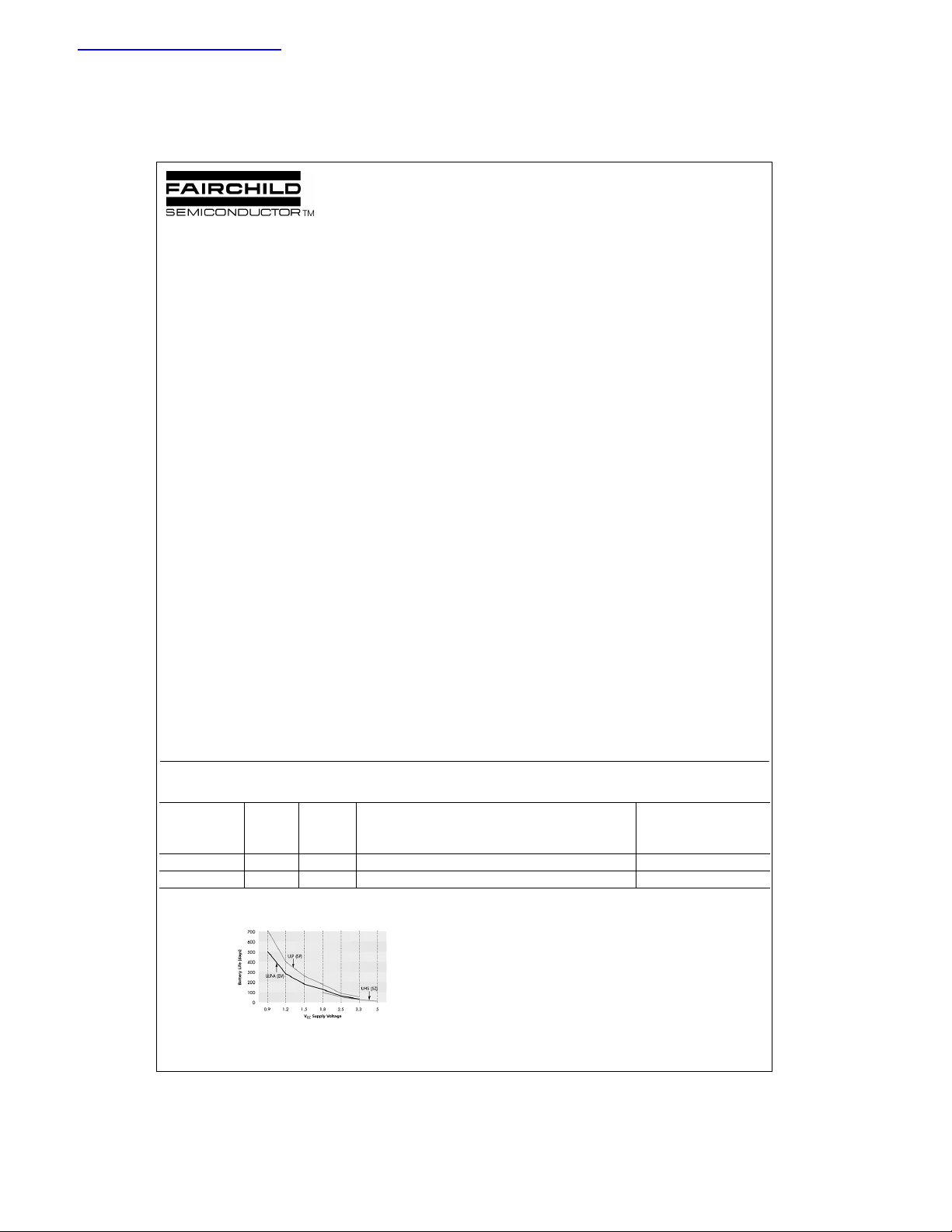
Battery Life vs. V
TinyLogic is a registered tradema rk of F airc hild Semiconduct or Corporation.
Quiet Series and MicroPak are trademarks of Fairchild Semiconductor Corporation.
Supply Voltage
CC
© 2004 Fairchild Semiconductor Corporation DS500808 www.fairchildsemi.com
Package Description Supplied AsPackage Code
TinyLogic ULP and ULP -A with up to 50% les s power consumption can
extend your battery lif e significantly.
Battery Life = (V
Where, P
device
Assumes ideal 3.6V Lithium Ion battery with current rating of 900mAH and
derated 90% and device freque nc y at 10MHz, with C
= (I
battery
*I
* VCC) + (C
CC
battery
*.9)/(P
PD
)/24hrs/day
device
+ CL) * V
CC
2
* f
= 15 pF load
L

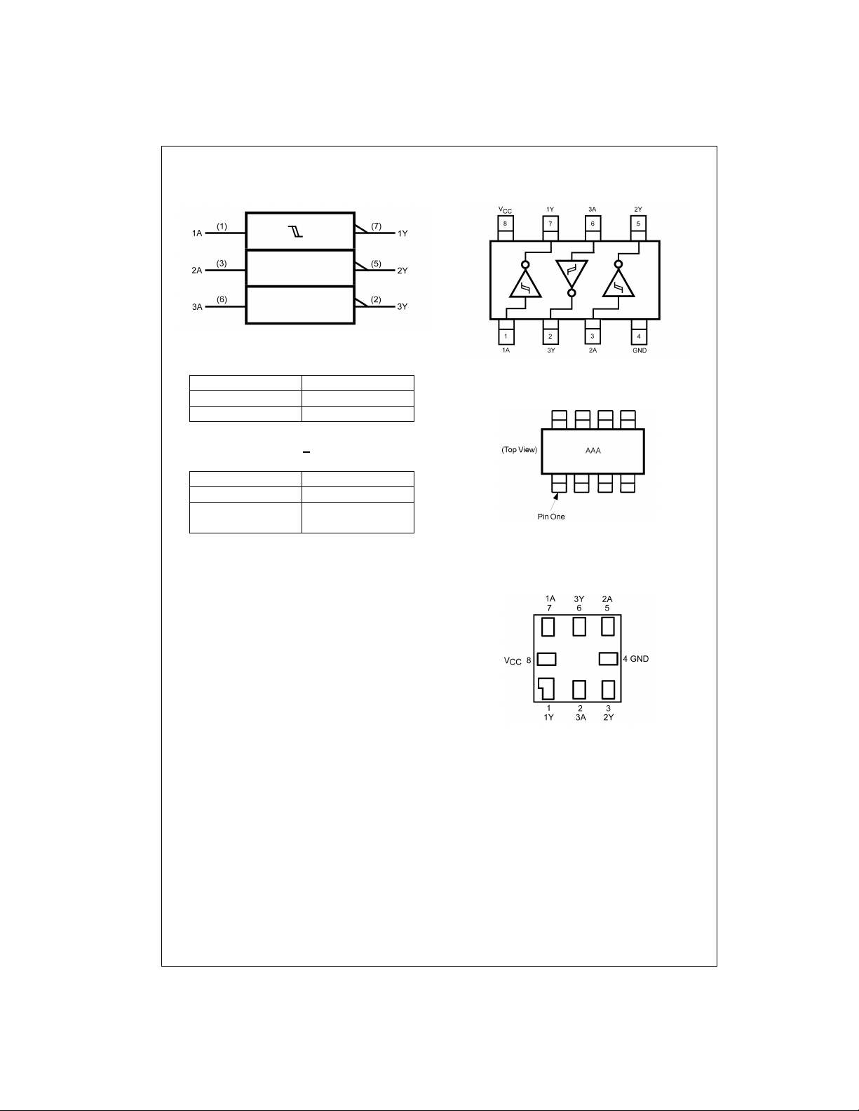
Logic Symbol
Connection Diagrams
NC7NP14
Pin Descriptions
Pin Names Description
A Input
Y Output
Function Table
Input Output
AY
LH
HL
H = HIGH Logic Level
L = LOW Logic Level
IEEE/IEC
Y = A
Pin Assignments f or US8
(Top View)
Pin One Orientation Diagram
AAA represents Product Code Top Mark - see ordering cod e
Note: Orientation of Top Mark determines Pin On e locat ion. Rea d the Top
Product Code Mark left to right, Pin One is the lower left pin (see diagram).
Pad Assignments for MicroPak
www.fairchildsemi.com 2
(Top Thru View)

Absolute Maximum Ratings(Note 1) Recommended Operating
Supply Voltage (VCC) −0.5V to +4.6V
DC Input Voltage (V
DC Output Voltage (V
HIGH or LOW State (Note 2)
V
= 0V −0.5V to 4.6V
CC
DC Input Diode Current (I
DC Output Diode Current (I
V
< 0V −50 mA
OUT
V
> V
OUT
CC
DC Output Source/Sink Current (I
DC V
or Ground Current per
CC
Supply Pin (I
Storage Temperature Range (T
) −0.5V to +4.6V
IN
)
OUT
) VIN < 0V ±50 mA
IK
)
OK
or Ground) ± 50 mA
CC
STG
−0.5V to V
) ± 50 mA
OH/IOL
CC
) −65°C to +150°C
+0.5V
+50 mA
Conditions
Supply Voltage 0.9V to 3.6V
Input Voltage (V
Output Voltage (V
HIGH or LOW State 0V to V
VCC = 0V 0V to 3.6V
Output Current in I
VCC = 3.0V to 3.6V ±2.6 mA
V
= 2.3V to 2.7V ±2.1 mA
CC
V
= 1.65V to 1.95V ±1.5 mA
CC
= 1.40V to 1.60V ±1.0 mA
V
CC
V
= 1.10V to 1.30V ±0.5 mA
CC
V
= 0.9V ±20 µA
CC
Free Air Operating Temperature (T
Minimum Input Edge Rate (
V
= 0.8V to 2.0V, VCC = 3.0V 10 ns/V
IN
Note 1: Absolute Maximum Ratings: are those values beyond which the
safety of the device can not be gu arant eed. The de vice sh ould no t be operated at these limits. The parametric values defined in the Electrical Characteristics tables are not guaranteed at the absolute maximum ratings. The
“Recommended Operating Con ditions” table will define the conditions for
actual device opera tion.
Absolute Maximum Rating must be observed.
Note 2: I
O
Note 3: Unused inputs must be held HIGH or LOW. They may not float.
(Note 3)
) 0.0V to 3.6V
IN
)
OUT
OH/IOL
) −40°C to +85°C
A
∆t/∆V)
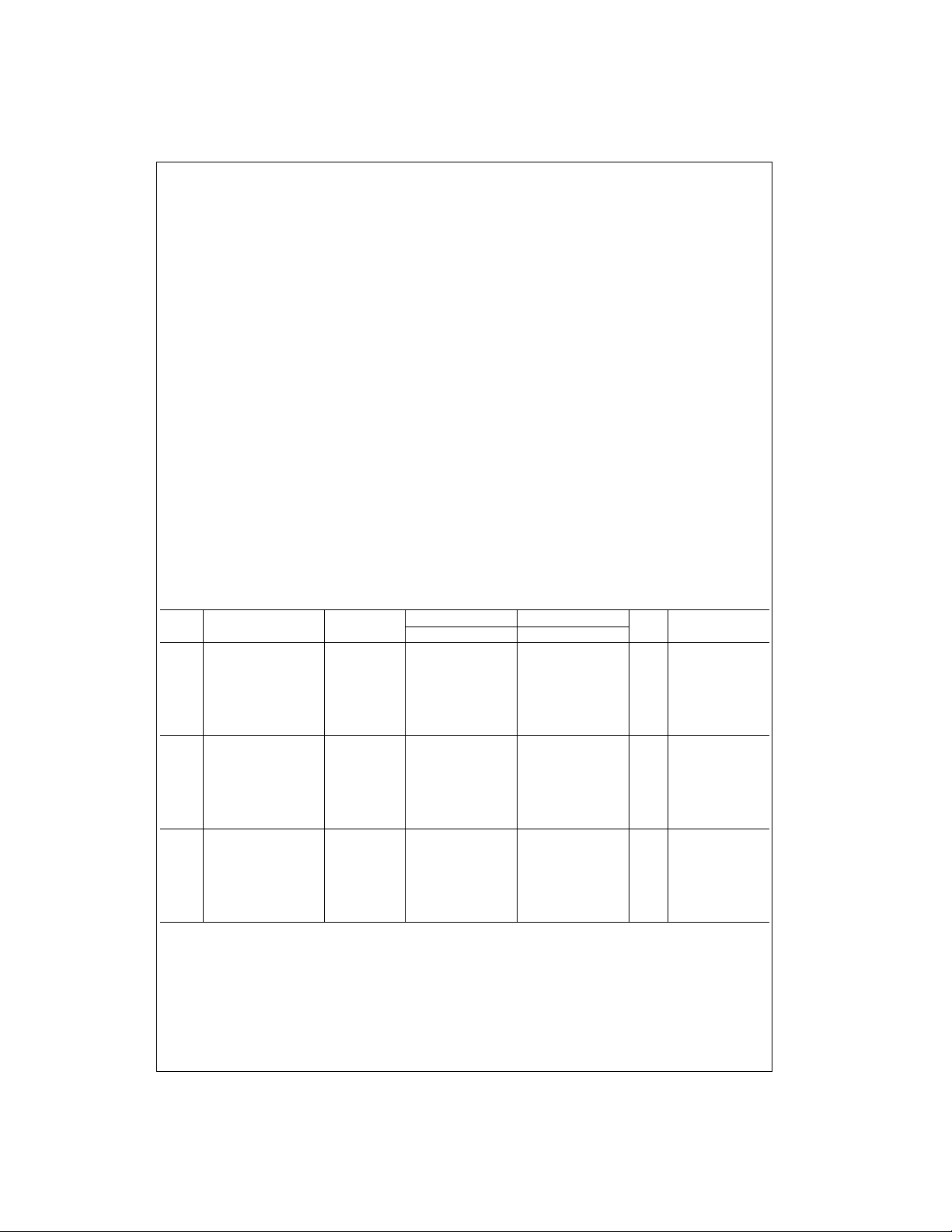
DC Electrical Characteristics
V
Symbol Parameter
V
Positive Threshold Voltage 0.90 0.3 0.6 0.3 0.6
P
V
Negative Threshold Voltage 0.90 0.1 0.6 0.1 0.6
N
V
Hysteresis Voltage 0.90 0.07 0.5 0.07 0.5
H
CC
(V) Min Max Min Max
1.10 0.4 1.0 0.4 1.0
1.40 0.5 1.2 0.5 1.2
1.65 0.7 1.5 0.7 1.5
2.30 1.0 1.9 1.0 1.9
3.00 1.5 2.6 1.5 2.6
1.10 0.15 0.7 0.15 0.7
1.40 0.2 0.8 0.2 0.8
1.65 0.25 0.9 0.25 0.9
2.30 0.4 1.15 0.4 1.15
3.00 0.6 1.5 0.6 1.5
1.10 0.08 0.6 0.08 0.6
1.40 0.09 0.8 0.09 0.8
1.65 0.10 1.0 0.10 1.0
2.30 0.25 1.1 0.25 1.1
3.00 0.60 1.8 0.60 1.8
TA = +25°CT
= −40°C to +85°C
A
Units Conditions
V
V
V
NC7NP14
CC
3 www.fairchildsemi.com
 Loading...