Fairchild MMBFJ305 service manual

MMBFJ305
N-Channel RF Amplifier
MMBFJ305 — N-Channel RF Amplifier
July 2011
Features
• This device is designed primarily for electronic switching
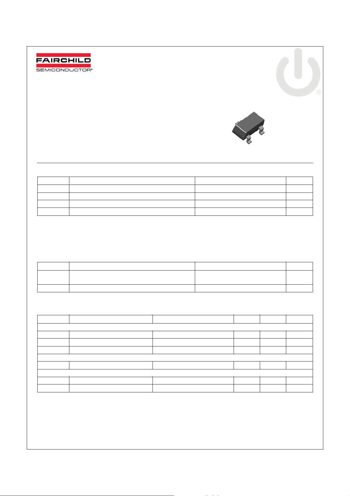
SOT-23
G
S
applications such as low On Resistance analog switching.
• Sourced from process 50.
Absolute Maximum Ratings* T
= 25°C unless otherwise noted
A
D
Note : Drain & Source are interchangeable.
Marking : 6Q
Symbol Parameter Value Units
V
DG
V
GS
I
GF
T
J, TSTG
* These ratings are limiting values above which the serviceability of any semiconductor device may be impaired.
NOTES:
1) These ratings are based on a maximum junction temperature of 150 degrees C.
2) These are steady state limits. The factory should be consulted on applications involving pulsed or low duty cycle
operations.
Thermal Characteristics* T
Drain-Gate Voltage 30 V
Gate-Source Voltage -30 V
Forward Gate Current 10 mA
Operating and Storage Junction Temperature Range -55 to +150 °C
= 25°C unless otherwise noted
A
Symbol Parameter Value Units
P
R
θJA
* Device mounted on FR-4 PCB 1.6” x 1.6” x 0.06”.
Total Device Dissipation
D
Derate above 25°C
225
1.8
Thermal Resistance, Junction to Ambient 556 °C/W
mW
mW/°C
Electrical Characteristics T
=25°C unless otherwise noted
A
Symbol Parameter Conditions Min. Max. Units
Off Characteristics
V
(BR)GSS
I
GSS
V
GS
On Characteristics
I
DSS
Small Signal Characteristics
gfs Forward Transfer Conductance V
g
OSS
* Pulse Test: Pulse Width ≤ 300μs, Duty Cycle ≤ 2.0%
© 2011 Fairchild Semiconductor Corporation www.fairchildsemi.com
MMBFJ305 Rev. A0 1
Gate-Source Breakdown Voltage IG = -1.0μA, VDS = 0 -30 V
Gate Reverse Current VGS = -20V, VDS = 0 -100 pA
(off) Gate-Source Cutoff Voltage VDS = 15V, ID = 1.0nA -0.5 -3.0 V
Zero-Gate Voltage Drain Current* VDS = 15V, VGS = 0 1.0 8.0 mA
= 15V, VGS = 0, f = 1.0kHz 3000 μmhos
DS
Output Conductance VDS = 15V, VGS = 0, f = 1.0kHz 50 μmhos

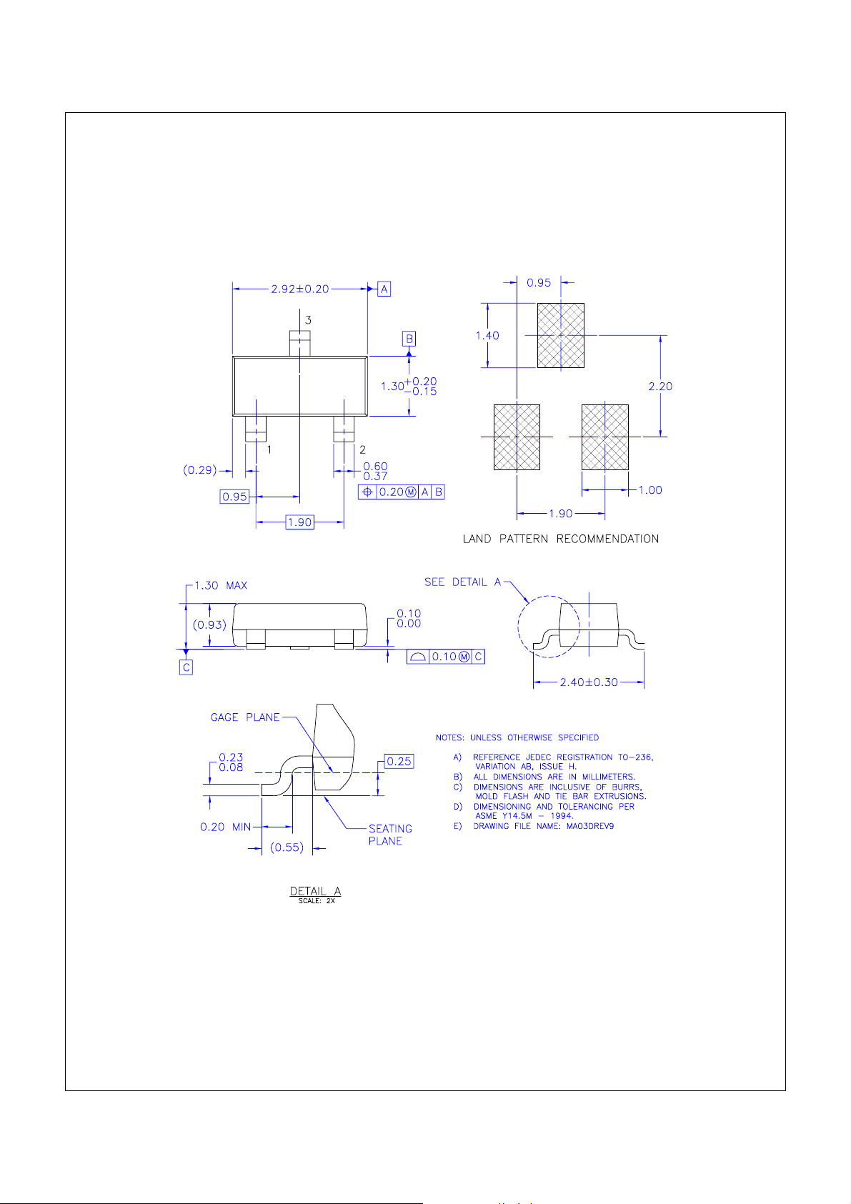
Physical Dimensions
MMBFJ305 — N-Channel RF Amplifier
SOT-23
Dimensions in Millimeters
© 2011 Fairchild Semiconductor Corporation www.fairchildsemi.com
MMBFJ305 Rev. A0 2
 Loading...