

September 1983
Revised May 2005
MM74HC540 • MM74HC541
Inverting Octal 3-STATE Buffer • Octal 3-STATE Buffer
MM74HC540 • MM74HC541 Inverting Octal 3-STATE Buffer • Octal 3-STATE Buffer
General Description
The MM74HC540 and MM74HC541 3-STATE buffers utilize advanced silicon-gate CMOS technology. They possess high drive current outp uts which enable high speed
operation even when driving large bus capacitances.
These circuits achieve speed s comparable to low power
Schottky devices, while r etaining the advantage of CMOS
circuitr y, i.e., high noise immuni ty, and low power consump tion. Both devices have a fano ut of 15 LS-TTL equivalent
inputs.
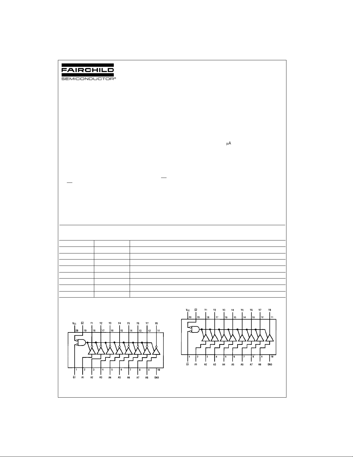
The MM74HC540 is an inverting buffer and the
MM74HC541 is a non-inverti ng buffer. The 3-STATE control gate operates as a two-input NOR such that if either G1
or G2 are HIGH, all eigh t outputs are in the high-impedance state.
In order to enhance PC board layout, the MM74HC540 and
MM74HC541 offers a pino ut having inputs a nd outputs on
opposite sides of the package. All inputs are protected from
damage due to static discharge by diodes to V
ground.
CC
Features
■ Typical propagation delay: 12 ns
■ 3-STATE outputs for connection to system buses
■ Wide power supply range: 2–6V
■ Low quiescent current: 80
■ Output current: 6 mA
and
P
A maximum (74HC Series)
Ordering Code:
Order Number Package Number Package Description
MM74HC540WM M20B 20-Lead Small Outline Integrated Circuit (SOIC), JEDEC MS-013, 0.300" Wide
MM74HC540SJ M20D 20-Lead Small Outline Package (SOP), EIAJ TYPE II, 5.3mm Wide
MM74HC540MTC MTC20 20-Lead Thin Shrink Small Outline Package (TSSOP), JEDEC MO-153, 4.4mm Wide
MM74HC540N N20A 20-Lead Plastic Dual-In-Line Package (PDIP), JEDEC MS-001, 0.300" Wide
MM74HC541WM M20B 20-Lead Small Outline Integrated Circuit (SOIC), JEDEC MS-013, 0.300" Wide
MM74HC541SJ M20D 20-Lead Small Outline Package (SOP), EIAJ TYPE II, 5.3mm Wide
MM74HC541MTC MTC20 20-Lead Thin Shrink Small Outline Package (TSSOP), JEDEC MO-153, 4.4mm Wide
MM74HC541N N20A 20-Lead Plastic Dual-In-Line Package (PDIP), JEDEC MS-001, 0.300" Wide
Devices also availab l e in Tape and Reel. Specify by appending the suffix let t er “X” to the ordering code.
Connection Diagrams
Pin Assignments for DIP, SOIC, SOP and TSSOP
Top View
MM74HC541
Top View
MM74HC540
© 2005 Fairchild Semiconductor Corporation DS005341 www.fairchildsemi.com
Absolute Maximum Ratings(Note 1)
(Note 2)
Supply Voltage (VCC)
DC Input Voltage (V
DC Output Voltage (V
Clamp Diode Current (I
DC Output Current, per pin (I
DC V
or GND Current,
CC
per pin (I
CC
)
IN
)
OUT
)
CD
OUT
)
Storage Temperature Range (T
Power Dissipation (P
MM74HC540 • MM74HC541
(Note 3) 600 mW
)
D
S.O. Package only 500 mW
Lead Temperature (T
)
L
(Soldering 10 seconds) 260
STG
1.5 to V
0.5 to V
)
)
65q
0.5 to 7.0V
CC
CC
r
20 mA
r
35 mA
r
70 mA
C to 150qC
Recommended Operating
Conditions
1.5V
0.5V
DC Input or Output Voltage
, V
(V
IN
OUT
Operating Temperature Range (T
Input Rise or Fall Times
, tf) V
(t
r
CC
V
CC
V
Supply Voltage (V
Note 1: Absolute Maximum Ratings a re those va lues beyon d which d amage to the device may occur.
Note 2: Unless otherwise specifie d all voltages are referenced to ground.
Note 3: Power Dissipation temp erature de rating — plastic “N” package:
12 mW/qC from 65qC to 85qC.
q
C
CC
)26V
CC
)0V
)4085qC
A
2.0V 1000 ns
4.5V 500 ns
6.0V 400 ns
Min Max Units
CC
DC Electrical Characteristics (Note 4)
TA
Symbol Parameter Conditions
V
Minimum HIGH Level 2.0V 1.5 1.5 1.5 V
IH
Input Voltage 4.5V 3.15 3.15 3.15 V
V
Maximum LOW Level 2.0V 0.5 0.5 0.5 V
IL
Input Voltage 4.5V 1.35 1.35 1.35 V
V
Minimum HIGH Level V
OH
Output Voltage |I
V
Maximum LOW Level V
OL
Output Voltage |I
I
Maximum Input V
IN
Current
I
Maximum 3-STATE V
OZ
Output Leakage V
Current
I
Maximum Quiescent V
CC
Supply Current I
Note 4: For a power supply of 5V r10% the worst ca se out put voltag es (VOH, and VOL) occur for HC a t 4.5V. Thus the 4.5V values s hould be used w hen
designing with this supply. Worst case V
, ICC, and IOZ) occur for CMOS at the higher voltage and so th e 6.0V values should be used.
rent (I
IN
VIH or V
IN
OUT
V
IN
|I
OUT
|I
OUT
IN
OUT
V
IN
|I
OUT
|I
OUT
IN
IN
OUT
IN
OUT
and VIL occur at V
IH
IL
| d 20 PA 2.0V 2.0 1.9 1.9 1.9 V
VIH or V
IL
| d 6.0 mA 4.5V 4.2 3.98 3.84 3.7 V
| d 7.8 mA 6.0V 5.7 5.48 5.34 5.2 V
VIH or V
IL
| d 20 PA 2.0V 0 0.1 0.1 0.1 V
VIH or V
IL
| d 6.0 mA 4.5V 0.2 0.26 0.33 0.4 V
| d 7.8 mA 6.0V 0.2 0.26 0.33 0.4 V
VCC or GND 6.0V
VIH or VIL, G VIH6.0V
VCC or GND
VCC or GND 6.0V 8.0 80 160
0 PA
CC
V
CC
6.0V 4.2 4.2 4.2 V
6.0V 1.8 1.8 1.8 V
4.5V 4.5 4.4 4.4 4.4 V
6.0V 6.0 5.9 5.9 5.9 V
4.5V 0 0.1 0.1 0.1 V
6.0V 0 0.1 0.1 0.1 V
5.5V and 4.5V respectively. (The VIH value at 5.5V is 3.85V.) The worst case leakage c ur-
25qCTA
Typ Guaranteed Limits
r
0.1
r
0.5
40 to 85qCTA
r
1.0
r
5
55 to 125qC
r
1.0
r
10
V
Units
P
P
P
A
A
A
www.fairchildsemi.com 2
AC Electrical Characteristics
V
5V, T
25qC, t
t
CC
A
6 ns
r
f
Symbol Parameter Conditions Typ
t
PHL
, t
PLH
Maximum Propagation CL
45 pF 12 18 ns
Delay (540)
t
PHL
, t
PLH
Maximum Propagation CL
45 pF 14 20 ns
Delay (541)
t
t
PZH
PHZ
, t
PZL
, t
PLZ
Maximum Output Enable RL
Time CL
Maximum Output Disable RL
Time CL
1 k
45 pF
1 k
5 pF
:
:
AC Electrical Characteristics
V
2.0V to 6.0V, C
CC
Symbol Parameter Conditions
t
, t
Maximum Propagation CL
PHL
PLH
Delay (540) C
t
, t
Maximum Propagation CL
PHL
PLH
Delay (541) C
t
, t
Maximum Output Enable RL
PZH
PZL
Time C
, t
t
Maximum Output Disable RL
PHZ
PLZ
Time CL
t
, t
Maximum Output Rise CL
THL
TLH
and Fall Time 4.5V 7 12 15 18 ns
C
Power Dissipation G V
PD
Capacitance (Note 5) G V
C
Maximum Input 5 10 10 10 pF
IN
Capacitance
C
Maximum Output Capacitance 15 20 20 20 pF
OUT
Note 5: CPD determines the no load dynamic power consumption, P
CPDVCCf ICC.
I
S
L
50 pF, t
t
6 ns (unless otherwise specified)
r
f
V
CC
TA
25qCTA
Typ Guaranteed Limits
50 pF 2.0V 55 100 126 149 ns
150 pF 2.0V 83 150 190 224 ns
L
CL
50 pF 4.5V 12 20 25 30 ns
C
150 pF 4.5V 22 30 38 45 ns
L
50 pF 6.0V 11 17 21 25 ns
C
L
CL
150 pF 6.0V 18 26 32 38 ns
50 pF 2.0V 58 115 145 171 ns
150 pF 2.0V 83 165 208 246 ns
L
CL
50 pF 4.5V 14 23 29 34 ns
C
150 pF 4.5V 17 33 42 49 ns
L
50 pF 6.0V 11 20 25 29 ns
C
L
CL
150 pF 6.0V 14 28 35 42 ns
1 k
:
50 pF 2.0V 75 150 189 224 ns
L
CL
150 pF 2.0V 100 200 252 298 ns
C
50 pF 4.5V 15 30 38 45 ns
L
150 pF 4.5V 30 40 50 60 ns
C
L
CL
50 pF 6.0V 13 26 32 38 ns
C
150 pF 6.0V 17 34 43 51 ns
L
1 k
:
2.0V 75 150 189 224 ns
50 pF 4.5V 15 30 38 45 ns
6.0V 13 26 32 38 ns
50 pF 2.0V 25 60 75 90 ns
6.0V 6 10 13 15 ns
IH
IL
CPD V
D
10 pF
50 pF
2
f ICC VCC, and the no load dynam ic cu rrent consumption,
CC
Guaranteed
Limit
Units
17 28 ns
15 25 ns
40 to 85qCTA
55 to 125qC
MM74HC540 • MM74HC541
Units
3 www.fairchildsemi.com

Physical Dimensions inches (millimeters) unless otherwise noted
MM74HC540 • MM74HC541
20-Lead Small Outline Integrated Circuit (SOIC), JEDEC MS-013, 0.300" Wide
Package Number M20B
www.fairchildsemi.com 4

Physical Dimensions inches (millimeters) unless otherwise noted (Continued)
MM74HC540 • MM74HC541
20-Lead Small Outline Package (SOP), EIAJ TYPE II, 5.3mm Wide
Package Number M20D
5 www.fairchildsemi.com

Physical Dimensions inches (millimeters) unless otherwise noted (Continued)
MM74HC540 • MM74HC541
20-Lead Thin Shrink Small Outline Package (TSSOP), JEDEC MO-153, 4.4mm Wide
www.fairchildsemi.com 6
Package Number MTC20

Physical Dimensions inches (millimeters) unless otherwise noted (Continued)
MM74HC540 • MM74HC541 Inverting Octal 3-STATE Buffer • Octal 3-STATE Buffer
20-Lead Plastic Dual-In-Line Package (PDIP), JEDEC MS-001, 0.300" Wide
Fairchild does not assume any responsibility for use of any circ uitry described, no circuit patent licenses are implied and
Fairchild reserves the right at any time without notice to change said circuitry and specifications.
LIFE SUPPORT POLICY
FAIRCHILD’S PRODUCTS ARE NOT AUTHORIZED FOR USE AS CRITICAL COMPONENTS IN LIFE SUPPORT
DEVICES OR SYSTEMS WITHOUT THE EXPRESS WRITTEN APPROVAL OF THE PRESIDENT OF FAIRCHILD
SEMICONDUCTOR CORPORATION. As used herein:
1. Life support devices or systems are dev ic es or syste ms
which, (a) are intended for surgical implant into the
body, or (b) support or sustain life, and (c) whose failure
to perform when properly used in accordance with
instructions for use provide d in the l abe ling, can be reasonably expected to result in a significant injury to the
user.
Package Number N20A
2. A critical compo nent in any com ponen t of a life s upp ort
device or system whose failure to perform can be reasonably expected to cause the failure of the life support
device or system, or to affect its safety or effectiveness.
www.fairchildsemi.com
7 www.fairchildsemi.com
 Loading...