Fairchild KMMBT5401, KMMBT5401 Schematic [ru]

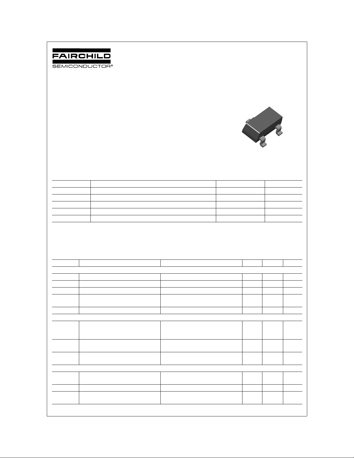
MMBT5401
PNP General Purpose Amplifier
• This device is designed as a general purpose amplifier and switch for
applications requiring high voltage.
PNP Epitaxial Silicon Transistor
MMBT5401
C
E
B
SOT-23
Mark: 2L
Absolute Maximum Ratings*
Ta=25°C unless otherwise noted
Symbol Parameter Value Units
V
CEO
V
CBO
V
EBO
I
C
, T
T
J
STG
* These ratings are limiting values above which the serviceability of any semiconductor device may be impaired.
Notes:
1. These ratings are based on a maximum junction temperature of 150 degrees C.
2. These are steady state limits. The factory should be consulted on applications involving pulsed or low duty cycle operations.
Electrical Characteristics
Collector-Emitter Voltage -150 V
Collector-Base Voltage -160 V
Emitter-Base Voltage -5.0 V
Collector Current - Continuous -600 mA
Operating and Storage Junction Temperature Range -55 ~ 150 °C
Ta=25°C unless otherwise noted
Symbol Parameter Test Condition Min. Max. Units
Off Characteristics
BV
BV
BV
I
CBO
I
EBO
CEO
CBO
EBO
Collector-Emitter Breakdown Voltage * IC = -1.0mA, IB = 0 -150 V
Collector-Base Breakdown Voltage IC = -100µA, IE = 0 -160 V
Emitter-Base Breakdown Voltage IE = -10µA, IC = 0 -5.0 V
Collector Cutoff Current V
= -120V, IE = 0
CB
= -120V, IE = 0, Ta = 100°C
V
CB
-50
-50
Emitter Cu to ff C u r re n t VEB= -3.0V, IC=0 -50 nA
On Characteristics *
h
FE
V
(sat) Collector-Emitter Saturation Voltage IC = -10mA, IB = -1.0mA
CE
(sat) Base-Emitter Saturation Voltage IC = -10mA, IB = -1.0mA
V
BE
DC Current Gain IC = -1.0mA, V
I
= -10mA, V
C
= -50mA, V
I
C
= -50mA, IB = -5.0mA
I
C
I
= -50mA, IB = -5.0mA
C
CE
CE
CE
= -5.0V
= -5.0V
= -5.0V
50
60
50
240
-0.2
-0.5
-1.0
-1.0
Small Signal Characterics
f
T
Current Gain Bandwidth Product IC = -10mA, V
= -10V,
CE
100 300 MHz
f = 100MHz
C
ob
N
F
* Pulse Test: Pulse Width ≤ 300µs, Duty Cycle ≤ 2.0%
Output Capacitance V
= -10V, IE = 0, f = 1MHz 6.0 pF
CB
Noise Figure IC = -250µA, V
f = 10Hz to 15.7KHz
= -5.0V, RS = 1.0KΩ
CE
8.0 d B
nA
µA
V
V
V
V
©2004 Fairchild Semiconductor Corporation Rev. B1, August 2004

MMBT5401
Thermal Characteristics
Symbol Parameter Max. Units
P
D
R
θJA
To tal Device Dissipation
Derate above 25°C
Thermal Resistance, Junction to Ambient 357 °C/W
Ta=25°C unless otherwise noted
350
2.8
mW
mW/°C
©2004 Fairchild Semiconductor Corporation
Rev. B1, August 2004

Typical Characteristics
Ω
β
β
Between Emitt er-Base
0.1 1 10 100 1000
170
180
190
200
210
220
RESISTANCE (k )
BV - BREAKDOWN VOLTAGE (V)
Ω
CER
β
MMBT5401
125 oC
25 oC
- 40 oC
200
VCE = 5V
150
125 oC
100
50
- TYPICAL PULSED CURRENT GAIN
0
FE
h
1E-4 1E-3 0.01 0.1 1
25 oC
- 40 oC
IC - COLLECTOR CURRENT (A)
0.4
ββββ
= 10
0.3
0.2
0.1
0.0
- COLLECTOR-EMITTER VOLTAGE (V)
0.1 1 10 100
CESAT
V
IC - COLLECTOR CURRENT (mA)
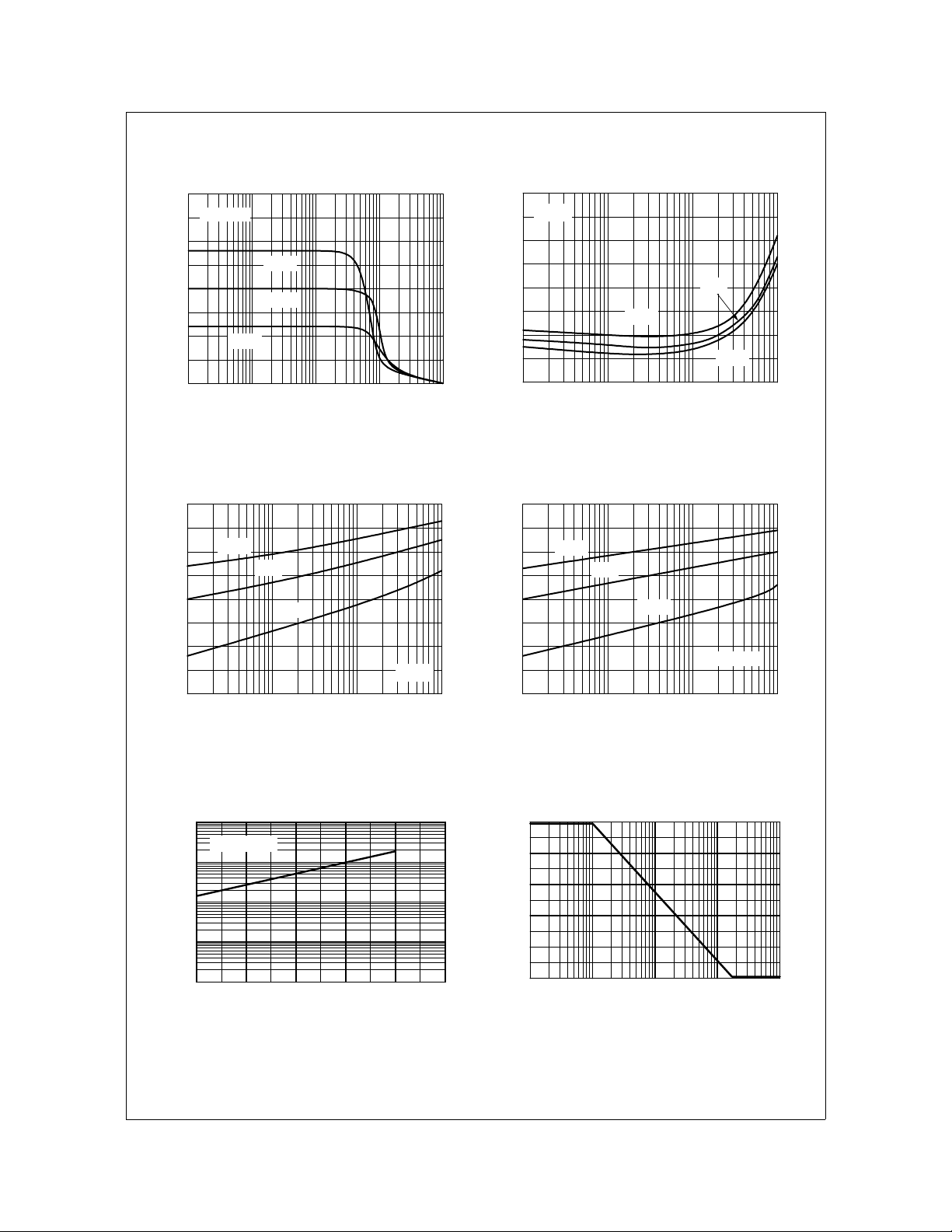
Figure 1. Typical Pulsed Current Gain
vs Collector Current
1.0
0.8
0.6
- 40 oC
25 oC
125 oC
Figure 2. Collector-Emitter Saturation
Voltage vs Collector Current
1.0
0.8
0.6
- 40 oC
25 oC
125 oC
0.4
- BASE-EMITTER VOLTAGE (V)
BESAT
0.2
V
0.1 1 10 100
Figure 3. Base-Emitter Saturation
Voltage vs Collector Current
100
V = 100V
CB
10
1
0.1
CBO
I - COLLECTOR CURRENT (nA)
25 50 75 100 125 150
Figure 5. Collector-Cutoff Current
IC - COLLECTOR CURRENT (mA)
T - AM BIEN T TE MPE RATU R E ( C)
A
vs Ambient Temperature
0.4
VCE = 5V
ββββ
= 10
- BASE-EMITTER ON VOLTAGE (V)
0.2
BC(ON)
0.1 1 10 100
V
IC - COLLECTOR CURRENT (mA)
Figure 4. Base-Emitter On Voltage vs
Collector Current
°
Figure 6. Collector-Emitter Breakdown Voltage
with Resistance Between Emitter-Base
©2004 Fairchild Semiconductor Corporation Rev. B1, August 2004
 Loading...