

Fairchild KA78LXXA, KA78L05AA service manual
查询KA78L05A供应商
KA78LXXA/KA78L05AA
3-Term inal 0.1A Positive Voltage Regulator
www.fairchildsemi.com
Features
• Maximum Output Current of 100mA
• Output Voltage of 5V, 6V, 8V, 9V,10V, 12V , 15V, 18V and
24V
• Thermal Overload Protection
• Short Circuit Current Limiting
• Output Voltage Offered in ±5% Tolerance
Description
The KA78LXXA/KA78L05AA s e ries of fixed vol tage
monolithic integrated circuit voltage regulators are suitable
for application that required supply current up to 100mA.
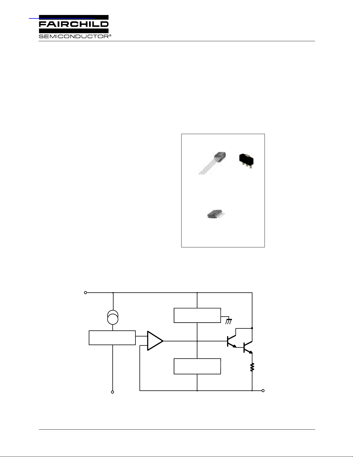
TO-92
2
1
3
1. Output 2. GND 3. Input
8-SOP
8
1. Output 2. GND 3. GND 4. NC
5. NC 6. GND 7. GND 8. Input
SOT-89
GND
1
2
3
1
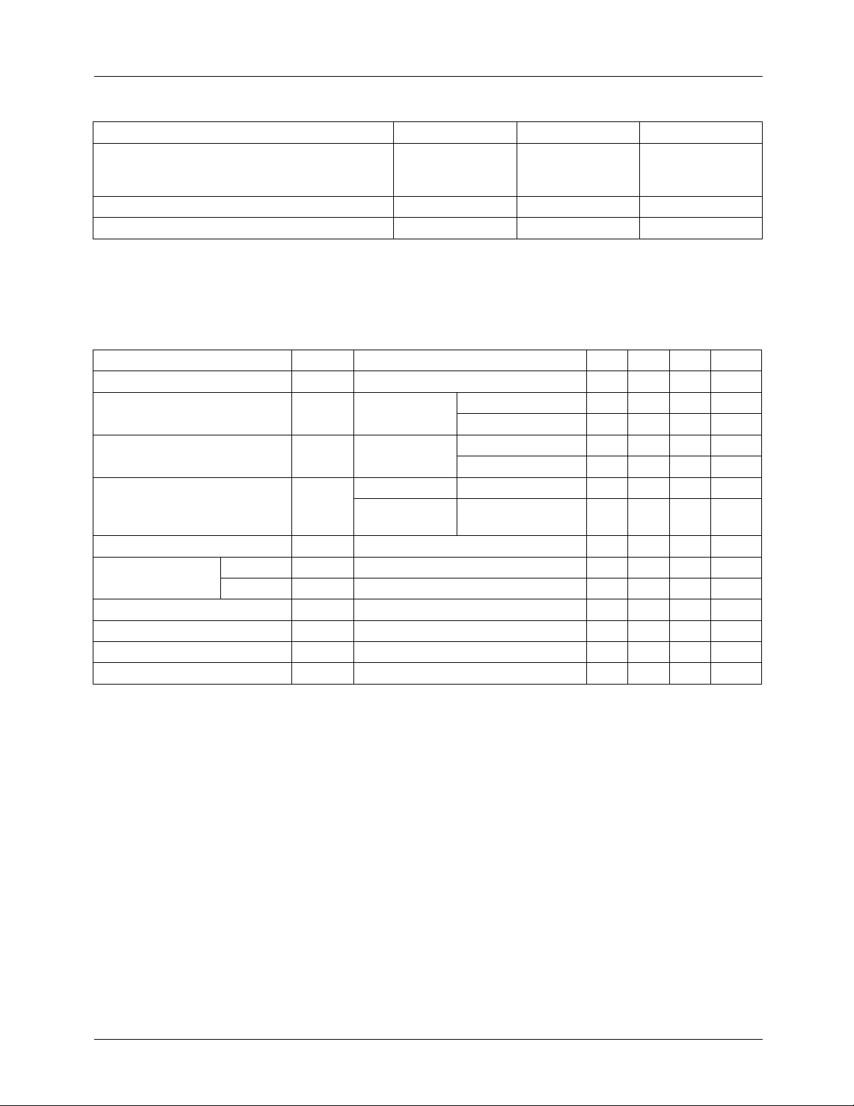
Internal Block Diagram
V
I
Inpu
t
3
REFERENCE VOLTAGE
GND
2
©2005 Fairchild Semiconductor Corporation
THERMAL SHUTDOWN
I
+
-
CIRCUIT
SHORT CIRCUIT
PROTECTION
R
SC
V
0
Outpu
t
1
Rev. 1.0.5
KA78LXXA/KA78L05AA
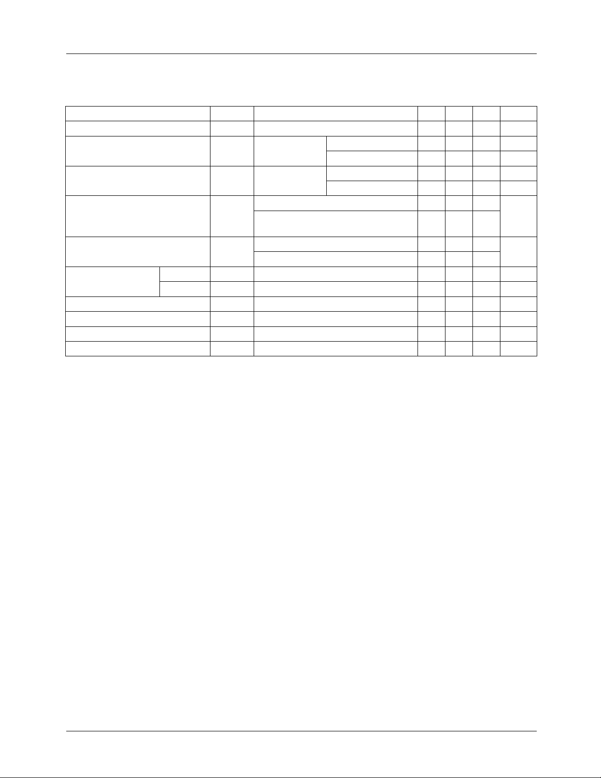
Absolute Maximum Ratings
Parameter Symbol Value Unit
Input Voltage (for V
(for V
= 12V to 18V)
O
(for V
O =
24V
= 5V, 8V)
O
Operating Junction Temperature Range T
Storage Temperature Range T
V
I
J
STG
30
35
40
0 ~ +150 °C
-65 ~ +150 °C
V
V
V
Electrical Characteristics(KA78L 0 5A)
(V
= 10V, I
I
Parameter Symbol Conditions Min. Typ. Max. Unit
Output Voltage V
Line Regulation (Note1)
Load Regulation (Note1)
Output Voltage V
Quiescent Current I
Quiescent Current
Change
Output Noise Voltage V
Temperature Coefficient of V
Ripple Rejection RR f = 120Hz, 8V ≤ V
Dropout Voltage V
= 40mA, 0°C ≤ TJ ≤ 125°C, CI = 0.33µF, CO = 0.1µF, unless otherwise specified. (Note1)
O
TJ = 25°C 4.8 5.0 5.2 V
O
∆V
∆V
O
O
TJ = 25°C
TJ = 25°C
7V ≤ V
8V ≤ V
1mA ≤ I
1mA ≤ I
≤ 20V - 8 150 mV
I
≤ 20V - 6 100 mV
I
≤ 100mA - 11 60 mV
O
≤ 40mA - 5.0 30 mV
O
7V ≤ VI ≤ 20V 1mA ≤ IO ≤ 40mA - - 5.25 V
With Line ∆I
With Load ∆I
∆VO/∆TIO = 5mA - -0.65 - mV/°C
O
O
7V ≤V
(Note2)
TJ = 25°C-2.05.5mA
Q
8V ≤VI ≤ 20V - - 1.5 mA
Q
1mA ≤ IO ≤ 40 mA - - 0.1 mA
Q
TA = 25°C, 10Hz ≤ f ≤ 100kHz - 40 - µV/Vo
N
TJ = 25°C-1.7-V
D
I
≤ V
MAX
1mA ≤ I
≤ 18V, TJ = 25°C4180 - dB
I
≤ 70mA 4.75 - 5.25 V
O
Note:
1. The max imum st eady sta te usable output cu rrent and inpu t voltage are very depende nt on the heat s inking an d/or l ead leng th
of the package. Th e data a bove rep resent p ulse tes t conditi ons with junction temper ature as indicated at the initiation o f test s.
2. Power dissipat ion P
≤ 0.75W.
D
2
KA78LXXA/KA78L05AA
Electrical Characteristics(KA78L 0 6A)
(V
I
= 12V, I
= 40mA, 0°C ≤ TJ ≤ 125°C, CI = 0.33µF, CO = 0.1µF, unless otherwise specified. (Note 1)
O
(Continued)
Parameter Symbol Conditions Min. Typ. Max. Unit
Output Voltage V
Line Regulation (Note1)
∆V
Load Regulation (Note1) ∆V
Output Voltage V
Quiescent Current I
Quiescent Current
Change
With Line ∆I
With Load ∆I
Output Noise Voltage V
Temperature Coefficient of V
∆VO/∆TIO = 5mA - 0.75 - mV/°C
O
Ripple Rejection RR f = 120Hz, 10V ≤ V
Dropout Voltage V
TJ = 25°C 5.75 6.0 6.25 V
O
O
O
TJ = 25°C
TJ = 25°C
8.5V ≤ V
9V ≤ V
1mA ≤ I
1mA ≤ I
≤ 20V - 64 175 mV
I
≤ 20V - 54 125 mV
I
≤ 100mA - 12.8 80 mV
O
≤ 70mA - 5.8 40 mV
O
8.5 ≤ VI ≤ 20V, 1mA ≤ IO ≤ 40mA 5.7 - 6.3 V
O
8.5 ≤ V
I
≤ V
(Note), 1mA ≤ IO ≤ 70mA 5.7 - 6.3 V
MAX
TJ = 25°C--5.5mA
Q
Q
Q
N
D
= 125°C-3.96.0mA
T
J
9 ≤ VI ≤ 20V - - 1.5 mA
1mA ≤ IO ≤ 40mA - - 0.1 mA
TA = 25°C, 10Hz ≤ f ≤ 100kHz - 40 - µV/Vo
≤ 20V, TJ = 25°C4046-dB
I
TJ = 25°C-1.7-V
Note:
1. The ma ximum ste ady stat e usable output current and input vo ltage ar e very d epende nt on th e heat s inking a nd/or lead le ngth
of the package. The dat a above repres ent pulse test c onditions with junction tempera ture as indica ted at the initi ation of test s.
2. Power dissipat ion P
≤ 0.75W.
D
3

KA78LXXA/KA78L05AA
Electrical Characteristics(KA78L 0 8A)
(V
I
= 14V, I
= 40mA, 0°C ≤ TJ ≤ 125°C, CI = 0.33µF, CO = 0.1µF, unless otherwise specified. (Note1)
O
(Continued)
Parameter Symbol Conditions Min. Typ. Max. Unit
Output Voltage V
Line Regulation (Note1)
∆V
Load Regulation (Note1) ∆V
TJ = 25°C 7.7 8.0 8.3 V
O
O
O
TJ = 25°C
TJ = 25°C
10.5V ≤ V
11V ≤ V
1mA ≤ I
1mA ≤ I
≤ 23V - 10 175 mV
I
≤ 23V - 8 125 mV
I
≤ 100mA - 15 80 mV
O
≤ 40mA - 8.0 40 mV
O
10.5V ≤ VI ≤ 23V 1mA ≤ IO ≤ 40mA 7.6 - 8.4 V
Output Voltage V
Quiescent Current I
Quiescent Current
Change
With Line ∆I
With Load ∆I
Output Noise Voltage V
Temperature Coefficient of V
O
Ripple Rejection RR f = 120Hz, 11V ≤ V
Dropout Voltage V
Note:
1. The max imum st eady sta te usable output cu rrent and inpu t voltage are very depende nt on the heat s inking an d/or l ead leng th
of the package. Th e data a bove rep resent p ulse tes t conditi ons with junction temper ature as indicated at the initiation o f test s.
2. Power dissipat ion P
≤ 0.75W.
D
O
10.5V ≤ V
V
MAX
TJ = 25°C-2.05.5mA
Q
11V ≤ VI ≤ 23V - - 1.5 mA
Q
1mA ≤ IO ≤ 40mA - - 0.1 mA
Q
TA = 25°C, 10Hz ≤ f ≤100kHz - 60 - µV/Vo
N
≤
I
(Note2)
1mA ≤ I
≤ 70mA 7.6 - 8.4 V
O
∆VO/∆TIO = 5mA - -0.8 - mV/°C
≤ 21V, TJ = 25°C39 70 - dB
I
TJ = 25°C-1.7-V
D
4
KA78LXXA/KA78L05AA
Electrical Characteristics(KA78L 0 9A)
(V
I
= 15V, I
= 40mA, 0°C ≤ TJ ≤ 125°C, CI = 0.33µF, CO = 0.1µF, unless otherwise specified. (Note1)
O
(Continued)
Parameter Symbol Conditions Min. Typ. Max. Unit
Output Voltage V
Line Regulation (Note1)
∆V
Load Regulation (Note1) ∆V
TJ = 25°C 8.64 9.0 9.36 V
O
O
O
TJ = 25°C
TJ = 25°C
11.5V ≤ V
13V ≤ V
1mA ≤ I
1mA ≤ I
≤ 24V - 90 200 mV
I
≤ 24V - 100 150 mV
I
≤ 100mA - 20 90 mV
O
≤ 40mA - 10 45 mV
O
11.5V ≤ VI ≤ 24V 1mA ≤ IO ≤ 40mA 8.55 - 9.45 V
Output Voltage V
Quiescent Current I
Quiescent Current
Change
With Line ∆I
With Load ∆I
Output Noise Voltage V
Temperature Coefficient of V
O
Ripple Rejection RR f = 120Hz, 12V ≤ V
Dropout Voltage V
Note:
1. The ma ximum ste ady stat e usable output current and input vo ltage ar e very d epende nt on th e heat s inking a nd/or lead le ngth
of the package. The dat a above repres ent pulse test c onditions with junction tempera ture as indica ted at the initi ation of test s.
2. Power dissipat ion P
≤ 0.75W.
D
O
11.5V ≤ V
V
MAX
TJ = 25°C-2.16.0mA
Q
13V ≤ VI ≤ 24V - - 1.5 mA
Q
1mA ≤ IO ≤ 40mA - - 0.1 mA
Q
TA = 25°C, 10Hz ≤ f ≤ 100kHz - 70 - µV/Vo
N
≤
I
(Note 2)
1mA ≤ I
≤ 70mA 8.55 - 9.45 V
O
∆VO/∆TIO = 5mA - -0.9 - mV/°C
≤ 22V, TJ = 25°C38 44 - dB
I
TJ = 25°C-1.7-V
D
5
KA78LXXA/KA78L05AA
Electrical Characteristics(KA78L 1 0A)
(V
I
= 16V, I
= 40mA, 0 °C ≤ TJ ≤ 125 °C, CI = 0.33 µF, CO = 0.1µF, unless otherwise specified. (Note1)
O
(Continued)
Parameter Symbol Conditions Min. Typ. Max. Unit
Output Voltage V
Line Regulation (Note1) ∆V
Load Regulation (Note1) ∆V
TJ = 25°C 9.6 10.0 10.4 V
O
O
O
TJ = 25°C
TJ = 25°C
12.5 ≤ V
14V ≤ V
1mA ≤ I
1mA ≤ I
≤ 25V - 100 220 mV
I
≤ 25V - 100 170 mV
I
≤ 100mA - 20 94 mV
O
≤ 70mA - 10 47 mV
O
12.5V ≤ VI ≤ 25V, 1mA ≤ IO ≤ 4 0 m A 9.5 - 10.5
Output Voltage V
Quiescent Current I
Quiescent Current
Change
With Line ∆I
With Load ∆I
Output Noise Voltage V
Temperature Coefficient of V
O
Ripple Rejection RR f = 120Hz, 15V ≤ V
Dropout Voltage V
O
12.5V ≤ V
1mA ≤ I
≤ V
I
≤ 70mA
O
MAX
(Note2)
9.5 - 10.5
TJ = 25°C - - 6.0
Q
Q
Q
N
=125°C-4.26.5
T
J
12.5 ≤ VI ≤ 25V - - 1.5 mA
1mA ≤ IO ≤ 40mA - - 0.1 mA
TA = 25°C, 10Hz ≤ f ≤ 100kHz - 74 - µV/Vo
∆VO/∆TIO = 5mA - 0.95 - mV/°C
≤ 25V, TJ = 25°C38 43 - dB
I
TJ = 25°C-1.7-V
D
V
mA
Notes:
1. The max imum st eady sta te usable output cu rrent and inpu t voltage are very depende nt on the heat s inking an d/or l ead leng th
of the package. Th e data a bove rep resent p ulse tes t conditi ons with junction temper ature as indicated at the initiation o f test s.
2. Power dissipat ion P
≤ 0.75W.
D
6
 Loading...