

KA5x03xx-SERIES
KA5H0365R, KA5M0365R, KA5L0365R
KA5H0380R, KA5M0380R, KA5L0380R
Fairchild Power Switch(FPS)
www.fairchildsemi.com
Features
• Precision Fixed Operating Frequency (100/67/50kHz)
• Low Start-up Current(Typ. 100uA)
• Pulse by Pulse Current Limiting
• Over Current Protection
• Over Voltage Protection (Min. 25V)
• Internal Thermal Shutdown Function
• Under Voltage Lockout
• Internal High Voltage Sense FET
• Auto-Restart Mode
Applications
• SMPS for VCR, SVR, STB, DVD & DVCD
• SMPS for Printer, Facsimile & Scanner
• Adaptor for Camcorder
Description
The Fairchild Power Switch(FPS) product family is specially
designed for an off-line SMPS with minimal external
components. The Fairchild Power Switch(FPS) consists of a
high voltage power SenseFET and a current mode PWM IC.
Included PWM controller integrates the fixed frequency
oscillator, the under voltage lock-out, the leading edge
blanking, the optimized gate turn-on/turn-off driver, the
thermal shutdown protection, the over voltage protection,
and the temperature compensated precision current sources
for the loop compensation and the fault protection circuitry.
Compared to a discrete MOSFET and a PWM controller or
an RCCsoluti on, a Fairchild Power Switch(FPS) can reduce
the total component count, design size and weight and at the
same time increase efficiency, productivity, and system
reliability. It has a basic platform well suited for the cost
effective design in either a flyback converter or a forward
converter
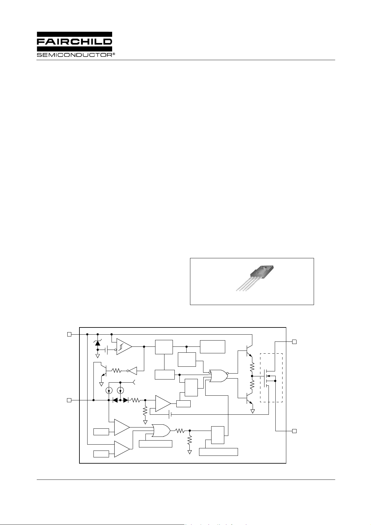
TO-220F-4L
1
1. GND 2. Drain 3. V
CC
4. FB
Internal Block Diagram
#3 V
CC
32V
μ
A
5
#4 FB
+
7.5V
27V
©2003 Fairchild Semiconductor Corporation
−
+
−
5V
Vref
OSC
9V
1mA
2.5R
1R
OVER VOLTAGE S/D
−
+
Thermal S/D
L.E.B
0.1V
Good
logic
S
R
Internal
bias
Q
S
R
Power on reset
#2 DRAIN
SFET
Q
#1 GND
Rev.1.0.7
KA5X03XX-SERIES
Absolute Maximum Ratings
(Ta=25°C, unless otherwise specified)
Characteristic Symbol Value Unit
KA5H0365R, KA5M0365R, KA5L0365R
Drain-Gate Voltage (R
=1MΩ)V
GS
Gate-Source (GND) Voltage V
Drain Current Pulsed
(1)
I
Continuous Drain Current (TC=25°C) I
Continuous Drain Current (TC=100°C) I
Single Pulsed Avalanche Energy
Maximum Supply Voltage V
(2)
E
CC,MAX
Analog Input Voltage Range V
Total Power Dissipation
Derating 0.6 W/°C
Operating Junction Temperature. T
Operating Ambient Temperature. T
Storage Temperature Range. T
KA5H0380R, KA5M0380R, KA5L0380R
Drain-Gate Voltage (R
=1MΩ)V
GS
Gate-Source (GND) Voltage V
Drain Current Pulsed
(1)
I
Continuous Drain Current (TC=25°C) I
Continuous Drain Current (TC=100°C) I
Single Pulsed Avalanche Energy
Maximum Supply Voltage V
(2)
E
CC,MAX
Analog Input Voltage Range V
Total Power Dissipation
Derating 0.6 W/°C
Operating Junction Temperature. T
Operating Ambient Temperature. T
Storage Temperature Range. T
DGR
GS
DM
D
D
AS
FB
P
D
J
A
STG
DGR
GS
DM
D
D
AS
FB
P
D
J
A
STG
650 V
±30 V
12.0 A
3.0 A
2.4 A
358 mJ
30 V
-0.3 to V
SD
75 W
+150 °C
-40 to +85 °C
-55 to +150 °C
800 V
±30 V
12.0 A
3.0 A
2.1 A
95 mJ
30 V
-0.3 to V
SD
75 W
+150 °C
-40 to +85 °C
-55 to +150 °C
DC
DC
DC
V
DC
DC
DC
V
Note:
1. Repetitive rating: Pulse width limited by maximum junction temperature
2. L = 51mH, starting Tj = 25°C
3. L = 13μH, starting Tj = 25°C
2
KA5X03XX-SERIES
Electrical Characteristics (SenseFET Part)
(Ta = 25°C unless otherwise specified)
Parameter Symbol Condition Min. Typ. Max. Unit
KA5H0365R, KA5M0365R, KA5L0365R
Drain-Source Breakdown Voltage BV
Zero Gate Voltage Drain Current I
Static Drain-Source on Resistance
Forward Transconductance
(Note)
(Note)
DSS
DSS
R
DS(ON)VGS
gfs VDS=50V, ID=0.5A 2.0 - - S
Input Capacitance Ciss
Reverse Transfer Capacitance Crss - 40 -
Turn On Delay Time td(on) V
Rise Time tr - 100 -
Turn Off Delay Time td(off) - 150 -
Fall Time tf - 42 -
Total Gate Charge
(Gate-Source+Gate-Drain)
Qg
Gate-Source Charge Qgs - 7.3 -
Gate-Drain (Miller) Charge Qgd - 13.3 -
VGS=0V, ID=50μA 650 - - V
VDS=Max. Rating, VGS=0V - - 50 μA
=0.8Max. Rating,
V
DS
V
=0V, TC=125°C
GS
- - 200 μA
=10V, ID=0.5A - 3.6 4.5 Ω
- 720 -
=0V, VDS=25V,
V
GS
f=1MHz
DD
=0.5BV
DSS
, ID=1.0A
- 150 (MOSFET switching
time is essentially
independent of
operating temperature)
V
=10V, ID=1.0A,
V
GS
DS
=0.5BV
(MOSFET
DSS
--34
switching time is essentially
independent of
operating temperature)
pFOutput Capacitance Coss - 40 -
nS
nC
KA5H0380R, KA5M0380R, KA5L0380R
Drain-Source Breakdown Voltage BV
DSS
VGS=0V, ID=50μA 800 - - V
VDS=Max. Rating, VGS=0V - - 250 μA
Zero Gate Voltage Drain Current I
Static Drain-Source on Resistance
Forward Transconductance
(Note)
(Note)
Input Capacitance Ciss
DSS
R
DS(ON)VGS
=0.8Max. Rating,
V
DS
V
=0V, TC=125°C
GS
- - 1000 μA
=10V, ID=0.5A - 4.0 5.0
gfs VDS=50V, ID=0.5A 1.5 2.5 - S
- 779 -
=0V, VDS=25V,
V
GS
f=1MHz
Reverse Transfer Capacitance Crss - 24.9 -
Turn On Delay Time td(on) V
Rise Time tr - 95 -
Turn Off Delay Time td(off) - 150 -
Fall Time tf - 60 -
Total Gate Charge
(Gate-Source+Gate-Drain)
Qg
Gate-Source Charge Qgs - 7.2 -
Gate-Drain (Miller) Charge
Note:
1. Pulse test: Pulse width ≤ 300μS, duty ≤ 2%
2.
1
--- -
S
=
R
Qgd - 12.1 -
=0.5BV
DD
(MOSFET switching
time is essentially
independent of
operating temperature)
V
=10V, ID=1.0A,
GS
V
=0.5BV
DS
switching time is
essentially independent of
operating temperature)
, ID=1.0A
DSS
(MOSFET
DSS
-40-
--34
Ω
pFOutput Capacitance Coss - 75.6 -
nS
nC
3
KA5X03XX-SERIES
Electrical Characteristics (Control Part) (Continued)
(Ta = 25°C unless otherwise specified)
Characteristic Symbol Test condition Min. Typ. Max. Unit
UVLO SECTION
Start Threshold Voltage V
Stop Threshold Voltage V
START
STOP
OSCILLATOR SECTION
Initial Accuracy F
Initial Accuracy F
Initial Accuracy F
Frequency Change With Temperature
(2)
OSC
OSC
OSC
--25°C≤Ta≤+85°C-±5 ±10 %
Maximum Duty Cycle Dmax
Maximum Duty Cycle Dmax
FEEDBACK SECTION
Feedback Source Current I
Shutdown Feedback Voltage V
FB
SD
Shutdown Delay Current Idelay Ta=25°C, 5V≤Vfb≤V
REFERENCE SECTION
Output Voltage
(1)
Temperature Stability
(1)(2)
Vref Ta=25°C 4.80 5.00 5.20 V
Vref/ΔT-25°C≤Ta≤+85°C-0.30.6mV/°C
CURRENT LIMIT(SELF-PROTECTION)SECTION
Peak Current Limit I
OVER Max. inductor current 1.89 2.15 2.41 A
PROTECTION SECTION
Over Voltage Protection V
Thermal Shutdown Temperature (Tj)
(1)
OVP
T
SD
TOTAL STANDBY CURRENT SECTION
Start-up Current I
Operating Supply Current
(Control Part Only)
START
I
OP
VFB=GND 14 15 16 V
VFB=GND 8.4 9 9.6 V
KA5H0365R
KA5H0380R
KA5M0365R
KA5M0380R
KA5L0365R
KA5L0380R
KA5H0365R
KA5H0380R
90 100 110 kHz
61 67 73 kHz
45 50 55 kHz
62 67 72 %
KA5M0365R
KA5M0380R
KA5L0365R
72 77 82 %
KA5L0380R
Ta=25°C, 0V<Vfb<3V 0.7 0.9 1.1 mA
Vfb>6.5V 6.9 7.5 8.1 V
SD
456μA
VCC>24V 25 27 29 V
- 140 160 - °C
VCC=14V - 100 170 μA
VCC<28 - 7 12 mA
Note:
1. These parameters, although guaranteed, are not 100% tested in production
2. These parameters, although guaranteed, are tested in EDS(water test) process
4
Typical Performance Characteristics(SenseFET part)
0
2
5
(KA5H0365R, KA5M0365R, KA5L0365R)
KA5X03XX-SERIES
10
V
GS
Top : 15V
10V
8.0V
7.0V
6.0V
5.5V
5.0V
Bottom :4.5V
1
, Drain Current [A]
D
I
0.1
110
@Notes:
1. 300 μs Pulse Test
2. TC = 25 oC
VDS, Drain-Source Voltage [V]
Figure 1. Output Characteristics
7
6
5
4
, [Ω ]
3
DS( on)
R
2
1
Drain-Source On-Resistance
0
012345
Vgs= 10V
Vgs= 20V
@ Note : Tj=25
ID,Drain Curre nt [A]
10
150 oC
1
, Drain Current [A]
D
I
0.1
o
25
C
24681
-25oC
@Not es :
1. VDS = 30V
2. 300 μs Pulse Test
VGS, Gate-Source Voltage [V]
Figure 2. Transfer Characteristics
1
0.1
℃
, Reverse Drain Current [A]
DR
I
0.01
0.40.60.81.01.
VSD, Source -Dra in Vol ta ge [V]
25 oC150 oC
@Notes :
1. VGS = 0 V
2. 300 μs Pulse Test
Figure 3. On-Resistance vs. Drain Current
700
C
= Cgs + Cgd (Cds = short ed)
600
500
400
300
Capacitance [pF]
200
100
0
10
C
iss
C
oss
C
rss
0
VDS, Drain-Source Voltage [V]
Figure 5. Capacitance vs. Drain-Source Voltage
iss
C
oss
C
rss
10
= Cds + C
= C
1
Figure 4. Source-Drain Diode Forward Voltage
10
gd
gd
8
6
4
,Gate-Source Voltage[V]
GS
2
V
0
0 5 10 15 20 2
Figure 6. Gate Charge vs. Gate-Source Volt age
VDS=130V
VDS=320V
VDS=520V
@ Note : ID=3.0A
QG,Total Gate Cha rge [n C]
5

KA5X03XX-SERIES
0
Typical Performance Characteristics (Continued)
(KA5H0365R, KA5M0365R, KA5L0365R)
1.2
1.1
1.0
, (Normalized)
DSS
BV
0.9
Drain-Source Breakdown Voltage
0.8
-50 0 50 100 150
TJ, Junction Temperature [oC]
Figure 7. Breakdown Voltage vs. Temperature
2
10
1
10
0
10
Operation in This Area
is Limited by R
DS(on)
10 ms
DC
@ Note s :
1. VGS = 0V
2. ID = 250μA
100 μs
1 ms
10 μs
2.5
2.0
1.5
, (Normalized)
1.0
DS(on )
R
Drain-Source On-Resistance
0.5
0.0
-50 0 50 100 150
TJ, Junction Temperature [oC]
Figure 8. On-Resistance vs. Temperature
3.0
2.5
2.0
1.5
@ Not es:
1. VGS = 10V
2. ID = 1.5 A
, Drain Current [A]
D
-1
10
I
-2
10
0
10
@ Notes :
1. T
C
2. T
J
3. Single Pulse
1
10
= 25 oC
= 150 oC
VDS , Drain-Source Voltage [V]
Figure 9. Max. Safe Operating Area
0
10
D=0.5
0.2
0.1
-1
10
0.05
(t) , Thermal Response
0.02
JC
θ
0.01
Z
-2
10
-5
10
1.0
, Drain Current [A]
D
I
0.5
2
10
3
10
0.0
25 50 75 100 125 15
TC, Case Temperature [oC]
Figure 10. Max. Drain Current vs. Case Temperature
@ Notes :
1. Z
2. Duty Factor, D=t1/t
(t)=1.25 oC/W Max.
JC
θ
3. TJM-TC=PDM*Z
single pulse
-4
10
-3
10
-2
10
-1
10
t1 , Square Wave Pulse Duration [sec]
Figure 11. Thermal Response
2
(t)
JC
θ
0
10
1
10
6

Typical Performance Characteristics (Continued)
(KA5H0380R, KA5M0380R, KA5L0380R)
KA5X03XX-SERIES
1
10
V
GS
T o p : 1 5 V
10 V
8.0 V
7.0 V
6.0 V
5.5 V
5.0 V
Bottom :4.5V
0
10
, Drain Current [A]
D
I
-1
10
0
10
@ N otes:
1. 3 00μs Pulse Test
2. TC = 25 oC
1
10
VDS, D rain-Source Voltage [V]
1
10
0
10
, D rain Current [A]
D
I
-1
10
150 oC
-25 oC25 oC
246810
@ Notes:
1. VDS = 30 V
2. 3 0 0 μs Pulse Test
VGS, G a te - S o u rc e Vo lta g e [V ]
Figure 1. Output Characteristics Figure 2. Thansfer Characteristics
8
7
6
5
4
, [Ω ]
D S( on)
3
R
2
Drain-Source On-R es istance
1
0
01234
Fig3. On-Res istance vs. D rain Current
Vgs= 10V
Vgs= 20V
@ N ote : T j= 25
ID,D ra in C urre n t
10
1
, R everse Drain Current [A]
DR
℃
I
0.1
150 oC
0.4 0.6 0.8 1.0
25 oC
VSD, Source-D rain Voltage [V]
Figure 3. On-Resistance vs. Drain Current Figure 4. Source-Drain Diode Forward Voltage
@ Notes:
1. VGS = 0V
2. 3 0 0 μs Pulse Test
1000
C
900
800
700
600
500
400
300
Capacitance [pF]
200
100
0
10
C
iss
C
oss
C
rs s
0
VDS, D rain-Source Voltage [V]
= Cgs + Cgd (Cds = shorted)
iss
C
= Cds + C
oss
C
gd
= C
rs s
gd
1
10
10
8
6
4
,Gate-Source Voltage[V]
GS
2
V
0
0 5 10 15 20 25 30
VDS=160V
VDS=400V
VDS= 640V
@ N ote : ID=3.0A
QG,Total Gate C harge [nC]
Figure 5. Capacitance vs. Drain-Source Voltage Figure 6. Gate Charge vs. Gate-Source Voltage
7

KA5X03XX-SERIES
Typical Performance Characteristics (Continued)
(KA5H0380R, KA5M0380R, KA5L0380R)
, (Normalized)
BV
1.2
1.1
1.0
DSS
0.9
Drain-Source Breakdown Voltage
0.8
-50 0 50 100 150
T
, Junction Temperature [oC]
J
@ Notes :
1. VGS = 0V
2. ID = 250μA
2.5
2.0
1.5
1.0
, (Normali zed)
DS(on)
R
0.5
Drain-Source On-Resistance
0.0
-50 0 50 100 150
TJ, Junction Temperature [oC]
@ Notes:
1. VGS = 10V
2. ID = 1.5 A
Figure 7. Breakdown Voltage vs. Temperature Figure 8. On-Resistance vs. Temperature
2
10
1
10
0
10
, Drain Current [A]
-1
D
10
I
-2
10
Operation in This Area
is Limited by R
@ Notes :
1. T
2. T
3. Single Pulse
1
10
= 25 oC
C
= 150 oC
J
DS(on)
DC
2
10
10 ms
1 ms
100 μs
10 μs
3
10
VDS , Drain-Source Voltage [V]
3.5
3.0
2.5
2.0
1.5
, Drain Current [A]
1.0
D
I
0.5
0.0
40 60 80 100 120 140
TC, Case Temperature [oC]
Figure 9. Max. Safe Operating Area
0
10
Figure 10. Max. Drain Current vs. Case Temperature
D=0.5
@ Notes :
0.2
0.1
-1
10
0.05
(t) , Thermal Response
Z
0.02
0.01
JC
θ
-2
10
-5
10
single pulse
-4
10
-3
10
10
1. Z
JC
θ
2. Duty Factor, D=t1/t
3. TJM-TC=PDM*Z
-2
-1
10
(t)=1.25 oC/W Max.
2
(t)
JC
θ
0
10
1
10
t1 , Square Wave Pulse Duration [sec]
Figure 11. Thermal Response
8

Typical Performance Characteristics (Control Part) (Continued)
(These characteristic graphs are normalized at Ta = 25°C)
KA5X03XX-SERIES
1.20
1.15
1.10
1.05
1.00
Fosc
0.95
0.90
0.85
0.80
-40 -25 0 25 50 75 100 125 150
Temperature [℃]
Figure 1. Operating Frequency
1.20
1.15
1.10
1.05
Iop
1.00
0.95
0.90
0.85
0.80
-40 -25 0 25 50 75 100 125 150
Temperature [℃]
1.20
1.15
1.10
1.05
Ifb
1.00
0.95
0.90
0.85
0.80
-40 -25 0 25 50 75 100 125 150
Temperature [℃]
Figure 2. Feedback Source Current
1.50
1.40
1.30
1.20
Iove r
1.10
1.00
0.90
0.80
0.70
-40 -25 0 25 50 75 100 125 150
Temperature [℃]
Figure 3. Operating Supply Current
1.30
1.20
1.10
1.00
Ista rt
0.90
0.80
0.70
0.60
-40 -25 0 25 50 75 100 125 150
Temperature [℃]
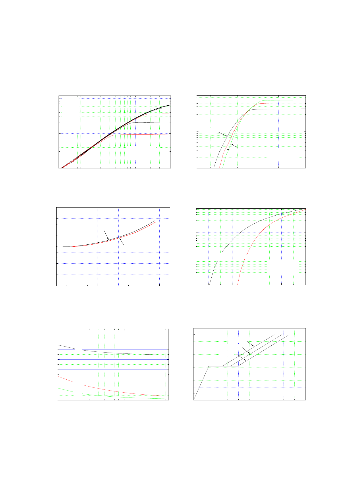
Figure 5. Start up Current
Figure 4. Peak Current Limit
1.20
1.15
1.10
1.05
Vstart
1.00
0.95
0.90
0.85
0.80
-40 -25 0 25 50 75 100 125 150
Temperature [℃]
Figure 6. Start Threshold Voltage
9

KA5X03XX-SERIES
Typical Performance Characteristics (Continued)
(These characteristic graphs are normalized at Ta = 25°C)
1.20
1.15
1.10
1.05
Vstop
1.00
0.95
0.90
0.85
0.80
-40 -25 0 25 50 75 100 125 150
Temperature [℃]
Figure 7. Stop Threshold Voltage
1.20
1.15
1.10
1.05
Vz
1.00
0.95
0.90
0.85
0.80
-40 -25 0 25 50 75 100 125 150
Temperature [℃]
1.20
1.15
1.10
1.05
1.00
Dmax
0.95
0.90
0.85
0.80
-40 -25 0 25 50 75 100 125 150
Temperature [℃]
Figure 8. Maximum Duty Cycle
1.20
1.15
1.10
1.05
1.00
Vsd
0.95
0.90
0.85
0.80
-40 -25 0 25 50 75 100 125 150
Temperature [℃]
Zener Voltage
CC
Idelay
Figure 9. V
1.20
1.15
1.10
1.05
1.00
0.95
0.90
0.85
0.80
-40 -25 0 25 50 75 100 125 150
Temperature [℃]
Figure 11. Shutdown Delay Current
Figure 10. Shutdown Feedback Voltage
1.20
1.15
1.10
1.05
Vovp
1.00
0.95
0.90
0.85
0.80
-40 -25 0 25 50 75 100 125 150
Temperature [℃]
Figure 12. Over Voltage Protection
10

Typical Performance Characteristics (Continued)
(These characteristic graphs are normalized at Ta = 25°C)
3.00
2.50
2.00
Rds(on)
1.50
1.00
0.50
0.00
-40 -25 0 25 50 75 100 125 150
Temperature [℃]
Figure13. Static Drain-Source on Resistance
KA5X03XX-SERIES
11

KA5X03XX-SERIES
Package Dimensions
TO-220F-4L
12

Package Dimensions (Continued)
TO-220F-4L(Forming)
KA5X03XX-SERIES
13

KA5X03XX-SERIES
Ordering Information
Product Number Package Marking Code BV
KA5H0365RTU TO-220F-4L
KA5H0365RYDTU TO-220F-4L(Forming)
KA5M0365RTU TO-220F-4L
KA5M0365RYDTU TO-220F-4L(Forming)
KA5L0365RTU TO-220F-4L
KA5L0365RYDTU TO-220F-4L(Forming)
5H0365R 650V 100kHz 3.6Ω
5M0365R 650V 67kHz 3.6Ω
5L0365R 650V 50kHz 3.6Ω
Product Number Package Marking Code BV
KA5H0380RTU TO-220F-4L
KA5H0380RYDTU TO-220F-4L(Forming)
KA5M0380RTU TO-220F-4L
KA5M0380RYDTU TO-220F-4L(Forming)
KA5L0380RTU TO-220F-4L
KA5L0380RYDTU TO-220F-4L(Forming)
TU :Non Forming Type
YDTU : Forming type
5H0380R 800V 100kHz 4.6Ω
5M0380R 800V 67kHz 4.6Ω
5L0380R 800V 50kHz 4.6Ω
DSS
DSS
F
F
OSC
OSC
R
DS(on)
R
DS(on)
DISCLAIMER
FAIRCHILD SEMICONDUCTOR RESERVES THE RIGHT TO MAKE CHANGES WITHOUT FURTHER NOTICE TO ANY
PRODUCTS HEREIN TO IMPROVE RELIABILITY, FUNCTION OR DESIGN. FAIRCHILD DOES NOT ASSUME ANY
LIABILITY ARISING OUT OF THE APPLICATION OR USE OF ANY PRODUCT OR CIRCUIT DESCRIBED HEREIN; NEITHER
DOES IT CONVEY ANY LICENSE UNDER ITS PATENT RIGHTS, NOR THE RIGHTS OF OTHERS.
LIFE SUPPORT POLICY
FAIRCHILD’S PRODUCTS ARE NOT AUTHORIZED FOR USE AS CRITICAL COMPONENTS IN LIFE SUPPORT DEVICES
OR SYSTEMS WITHOUT THE EXPRESS WRITTEN APPROVAL OF THE PRESIDENT OF FAIRCHILD SEMICONDUCTOR
CORPORATION. As used herein:
1. Life support devices or systems are devices or systems
which, (a) are intended for surgical implant into the body,
or (b) support or sustain life, and (c) whose failure to
perform when properly used in accordance with
instructions for use provided in the labeling, can be
reasonably expected to result in a significant injury of the
user.
www.fairchildsemi.com
2. A critical component in any component of a life support
device or system whose failure to perform can be
reasonably expected to cause the failure of the life support
device or system, or to affect its safety or effectiveness.
6/3/08 0.0m 001
© 2003 Fairchild Semiconductor Corporation
Stock#DSxxxxxxxx

®
®
TRADEMARKS
The following includes registered and unregistered trademarks and service marks, owned by Fairchild Semiconductor and/or its global subsidiaries, and is not
intended to be an exhaustive list of all such trademarks.
2Cool
AccuPower
Auto-SPM
AX-CAP*
®
BitSiC
Build it Now
CorePLUS
CorePOWER
CROSSVOLT
CTL
Current Transfer Logic
DEUXPEED
Dual Cool™
EcoSPARK
®
®
EfficientMax
ESBC
®
Fairchild
Fairchild Semiconductor
FACT Quiet Series
®
FACT
®
FAST
FastvCore
FETBench
FlashWriter
®
*
FPS
F-PFS
®
FRFET
Global Power ResourceSM
Green FPS
Green FPS e-Series
Gmax
GTO
IntelliMAX
ISOPLANAR
Making Small Speakers Sound Louder
and Better™
MegaBuck
MICROCOUPLER
MicroFET
MicroPak
MicroPak2
MillerDrive
®
MotionMax
Motion-SPM
mWSaver
OptoHiT
OPTOLOGIC
OPTOPLANAR
®
®
®
PDP SPM
Power-SPM
PowerTrench
®
PowerXS™
Programmable Active Droop
®
QFET
QS
Quiet Series
RapidConfigure
Saving our world, 1mW/W/kW at a time™
SignalWise
SmartMax
SMART START
®
SPM
STEALTH
SuperFET
®
SuperSOT-3
SuperSOT-6
SuperSOT-8
SupreMOS
®
SyncFET
Sync-Lock™
®
*
The Power Franchise
TinyBoost
TinyBuck
TinyCalc
TinyLogic
®
TINYOPTO
TinyPower
TinyPWM
TinyWire
®
TranSiC
TriFault Detect
TRUECURRENT
®
*
SerDes
®
UHC
Ultra FRFET
UniFET
VCX
VisualMax
VoltagePlus
XS™
* Trademarks of System General Corporation, used under license by Fairchild Semiconductor.
DISCLAIMER
FAIRCHILD SEMICONDUCTOR RESERVES THE RIGHT TO MAKE CHANGES WITHOUT FURTHER NOTICE TO ANY PRODUCTS HEREIN TO IMPROVE
RELIABILITY, FUNCTION, OR DESIGN. FAIRCHILD DOES NOT ASSUME ANY LIABILITY ARISING OUT OF THE APPLICATION OR USE OF ANY PRODUCT
OR CIRCUIT DESCRIBED HEREIN; NEITHER DOES IT CONVEY ANY LICENSE UNDER ITS PATENT RIGHTS, NOR THE RIGHTS OF OTHERS. THESE
SPECIFICATIONS DO NOT EXPAND THE TERMS OF FAIRCHILD’S WORLDWIDE TERMS AND CONDITIONS, SPECIFICALLY THE WARRANTY THEREIN,
WHICH COVERS THESE PRODUCTS.
LIFE SUPPORT POLICY
FAIRCHILD’S PRODUCTS ARE NOT AUTHORIZED FOR USE AS CRITICAL COMPONENTS IN LIFE SUPPORT DEVICES OR SYSTEMS WITHOUT THE
EXPRESS WRITTEN APPROVAL OF FAIRCHILD SEMICONDUCTOR CORPORATION.
As used herein:
1. Life support devices or systems are devices or systems which, (a)
are intended for surgical implant into the body or (b) support or
sustain life, and (c) whose failure to perform when properly used in
accordance with instructions for use provided in the labeling, can be
reasonably expected to result in a significant injury of the user.
2. A critical component in any component of a life support, device, or
system whose failure to perform can be reasonably expected to
cause the failure of the life support device or system, or to affect its
safety or effectiveness.
ANTI-COUNTERFEITING POLICY
Fairchild Semiconductor Corporation's Anti-Counterfeiting Policy. Fairchild's Anti-Counterfeiting Policy is also stated on our external website,
www.fairchildsemi.com, under Sales Support.
Counterfeiting of semiconductor parts is a growing problem in the industry. All manufacturers of semiconductor products are experiencing counterfeiting of their
parts. Customers who inadvertently purchase counterfeit parts experience many problems such as loss of brand reputation, substandard performance, failed
applications, and increased cost of production and manufacturing delays. Fairchild is taking strong measures to protect ourselves and our customers from the
proliferation of counterfeit parts. Fairchild strongly encourages customers to purchase Fairchild parts either directly from Fairchild or from Authorized Fairchild
Distributors who are listed by country on our web page cited above. Products customers buy either from Fairchild directly or from Authorized Fairchild Distributors
are genuine parts, have full traceability, meet Fairchild's quality standards for handling and storage and provide access to Fairchild's full range of up-to-date
technical and product information. Fairchild and our Authorized Distributors will stand behind all warranties and will appropriately address any warranty issues that
may arise. Fairchild will not provide any warranty cove rage or other assistance for parts bought from Unauthorized Sources. Fairchild is comm itted to combat this
global problem and encourage our customers to do their part in stopping this practice by buying direct or from authorized distributors.
PRODUCT STATUS DEFINITIONS
Definition of Terms
Datasheet Identification Product Status Definition
Advance Information Formative / In Design
Preliminary First Production
No Identification Needed Full Production
Obsolete Not In Production
Datasheet contains the design specifications for product development. Specifications may change
in any manner without notice.
Datasheet contains preliminary data; supplementary data will be published at a later date. Fairchild
Semiconductor reserves the right to make changes at any time without notice to improve design.
Datasheet contains final specifications. Fairchild Semiconductor reserves the right to make
changes at any time without notice to improve the design.
Datasheet contains specifications on a product that is discontinued by Fairchild Semiconductor.
The datasheet is for reference information only.
Rev. I57
© Fairchild Semiconductor Corporation www.fairchildsemi.com
 Loading...