

Datasheet KA431SAMF, KA431SAMF2, KA431SLMF, KA431SLMF2, KA431SMF Datasheet (Fairchild) [ru]
...
KA431S/KA431SA/KA431SL
Programmable Shunt Regulator
www.fairchildsemi.com
Features
• Programmable Output Voltage to 36 Volts
• Low Dynamic Output Impedance 0.20 Typical
• Sink Current Capability of 1.0 to 100mA
• Equivalent Full-Range Temperature Coefficient of
50ppm/°C Typical
• Tem perature Compensated for Operation Over Full Rated
Operating Temperature Range
• Low Output Noise Voltage
• Fast Turn-on Response
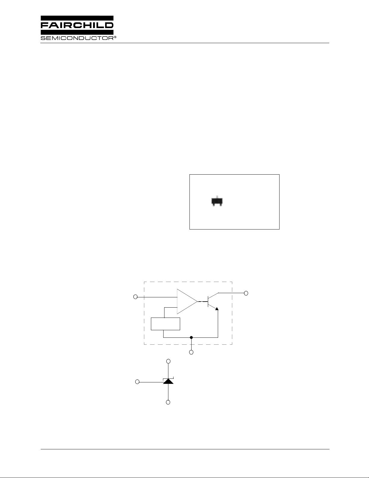
Internal Block Diagram
Description
The KA431S/KA431SA/KA431SL are three-terminal
adjustable regulator series with a guaranteed thermal
stability over applicable temperature ranges. The output
voltage may be set to any value between V
(approximately 2.5 volts) and 36 volts with two external
resistors These devices have a typical dynamic output
impedance of 0.2W Active output circuitry provides a very
sharp turn on characteristic, making these devices excellent
replacement for zener diodes in many applications.
SOT-23F
3
2
1
MF- 1.Cathode 2. Ref 3. Anode
MF2- 1. Ref 2. Cathode 3. Anode
REF
REFERENCE
REFERENCE (R)
©2005 Fairchild Semiconductor Corporation
2.5 Vref
+
-
ANODE
CATHODE (K)
ANODE(A)
CATHODE
Rev. 1.0.6
KA431S/KA431SA/KA431SL
Absolute Maximum Ratings
(Operating temperature range applies unless otherwise specified.)
Parameter Symbol Value Unit
Cathode Voltage V
Cathode Current Range (Continuous) I
Reference Input Current Range I
Thermal Resistance Junction-Air (Note1,2)
MF Suffix Package
Power Dissipation (Note3,4)
MF Suffix Package
Junction Temperature T
Operating Temperature Range T
Storage Temperature Range T
Note :
1. Thermal resistance test board
Size: 76.2mm * 114.3mm * 1.6mm (1S0P)
JEDEC Standard: JESD51-3, JESD51-7
2. Assume no ambient airflow.
3. T
JMAX
4. Power dissipation calculation: PD = (TJ - TA)/
= 150
°
C
, Ratings appl y to ambient te m perature at 25
R
θJA
REF
R
P
OPR
STG
°
C
KA
KA
θJA
D
J
37 V
-100 ~ +150 mA
-0.05 ~ +10 mA
350 °C/W
350 mW
150 °C
-25 ~ +85 °C
-65 ~ +150 °C
Recommended Operating Conditions
Parameter Symbol Min. Typ. Max. Unit
Cathode Voltage V
Cathode Current I
KA
KA
V
REF
-36V
1.0 - 100 mA
2
Electrical Characteristics
(TA = +25°C, unless otherwise specified)
KA431S/KA431SA/KA431SL
Parameter Symbol Conditions
Reference Input
Voltage
Deviation of
Reference
Input Voltage
OverTemperature
Ratio of Change
in Reference
Input Voltage
to the Change i n
Cathode
Voltage
Reference Input
Current
Deviation of
Reference
Input Current
Over Full
Temperature
Range
Minimum
Cathode Current for
Regulation
Off - Stage
Cathode
Current
Dynamic
Impedance ZKA
V
REF
∆VREF/∆TVKA=VREF,
∆VREF/
∆VKA
IREF
∆IREF/∆T
IKA(MIN) VKA=VREF - 0.45 1.0 - 0.45 1.0 - 0.45 1.0 mA
IKA(OFF)
VKA=V
REF
=10mA
I
KA
IKA=10mA
TMIN≤TA≤TMAX
∆VKA=10
IKA
=10mA
IKA=10mA,
R1=10kΩ,R2=∞
IKA=10mA,
R1=10kΩ,R2=∞
TA =Full Range
VKA=36V,
VREF=0
VKA=VREF,
IKA=1 to 100mA
f ≥1.0kHz
V-VREF
∆VKA=36
V-10V
KA431S KA431SA KA431SL
Min. Typ. Max. Min. Typ. Max. Min. Typ. Max.
,
2.450 2.500 2.550 2.470 2.495 2.520 2.482 2.495 2.508 V
-
4.5 17
- -1.0 -2.7 - -1.0 -2.7 - -1.0 -2.7
- -0.5 -2.0 - -0.5 -2.0 - -0.5 -2.0
-1.54 -1.54 -1.54
-
0.4 1.2
- 0.05 1.0 - 0.05 1.0 - 0 .05 1.0
- 0.15 0.5 - 0.15 0.5 - 0 .15 0.5 Ω
-
-
4.5 17
0.4 1.2
-
4.5 17 mV
-
0.4 1.2
Unit
mV/V
µ
A
µ
A
µ
A
•T
MIN
= -25°C, T
MAX
= +85°C
3

KA431S/KA431SA/KA431SL
Test Circuits
KA431S
Figure 1. Test Circuit for VKA=V
KA431S
Figure 3. Test Circuit for l
KA(OFF)
REF
KA431S
Figure 2. Test Circuit for V
KA≥VREF
4

Typical Performance Characteristics
KA431S/KA431SA/KA431SL
150
VKA = V
REF
TA = 25oC
100
50
0
, Cathode Current (mA)
K
I
-50
-100
-2-10123
Figure 4.
Cathode Current vs. Cathode Voltage
0.100
0.075
0.050
0.025
, Off-State Cathode Current (uA)
off
I
0.000
-50-250 255075100125
VKA, Cathode Voltage (V)
TA, Ambient Temperature (oC)
800
VKA = V
REF
TA = 25oC
600
400
200
, CATHODE CURRENT (uA)
KA
I
0
-200
-10123
Figure 5.
Cathode Current vs. Cathode Voltage
3.5
3.0
2.5
2.0
1.5
1.0
, Reference Input Current (uA)
ref
I
0.5
0.0
-50 -25 0 25 50 75 100 125
VKA, CATHODE VOLTAGE (V)
I
KA(MIN)
TA, Ambient Temperature (oC)
Figure 6.
OFF-State Cathode Current vs.
Figure7. Reference Input Current vs.
Ambient Temperature
60
50
40
30
20
Open Loop Voltage Gain (dB)
10
0
-10
1k 10k 100k 1M 10M
Frequency (Hz)
TA = 25oC
I
KA
= 10mA
6
TA=25oC
5
4
3
Voltage Swing (V)
2
1
0
048121620
Figure 8. Small Signal Voltage Amplification vs. Frequency Figure 9.
Ambient Temperature
INPUT
OUTPUT
Time (us)
Pulse Response
5

KA431S/KA431SA/KA431SL
Typical Performance Characteristics
140
120
100
80
60
40
, CATHODE CURRENT(mA)
K
I
20
0
100p 1n 10n 100n 1
A
stable
Figure 10. Stability Boundary Conditions
5
4
3
2
Current(mA)
B
CL, LOAD CAPACITANCE
A VKA = Vref
B V
= 5.0 V @ IK = 10
KA
TA = 25oC
stable
mA
!
10
!
(Continued)
5
4
3
2
Current(mA)
1
0
0.0 0.2 0.4 0.6 0.8 1.0 1.2 1.4 1.6 1.8 2.0
Anode-Ref. Voltage(V)
Figure 11. Anode-Reference Diode Curve
1
0
0.0 0.2 0.4 0.6 0.8 1.0 1.2 1.4 1.6 1.8 2.0
Ref.-Cathode Voltage(V)
Figure 12. Ref erence-Catho de Diode Curve
6

Typical Application
KA431S/KA431SA/KA431SL
R
1
------ -
V
V
Figure 13. Shunt Regulator
+
1
=
O
KA431S
ref
R
2
Figure 14
-
KA431S
Figure 16. Curren t Li mi t or Cu rrent Source
R
1
------ -
=
VOV
.
Output Control for
+
1
ref
R
KA431S
2
Three-Termianl Fixed Regulator
Figure 17. Constant-Current Sink
R
1
------ -
V
V
+
1
=
O
R
2
ref
KA431S
Figure 15. High Current Shunt Regulator
KA431S
7

KA431S/KA431SA/KA431SL
Mechanical Dimensions
Package
Dimensions in millimeters
SOT-23F
8

Marking
KA431S/KA431SA/KA431SL
MF-
MF2-
43A
43B
43C
2% tolerance 1% tolerance 0.5% tolerance
43D
43A
43E
43B
43F
43C
2% tolerance 1% tolerance 0.5% tolerance
9

KA431S/KA431SA/KA431SL
Ordering Information
Product Number Output Voltage Tolerance Package Operating Temperature
KA431SLMF 0.5% SOT-23F
KA431SAMF 1% SOT-23F
KA431SMF 2% SOT-23F
KA431SLMF2 0.5% SOT-23F
KA431SAMF2 1% SOT-23F
KA431SMF2 2% SOT-23F
-25 ~ +85°C
DISCLAIMER
FAIRCHILD SEMICONDUCTOR RESERVES THE RIGHT TO MAKE CHANGES WITHOUT FURTHE R NOTICE TO ANY
PRODUCTS HEREI N TO IMPROVE RELIAB ILITY, FUNCTION OR DESIGN. FAIRCHILD DOES NOT ASSUME AN Y
LIABILITY ARISING OUT OF THE APPLICATION OR USE OF ANY PRODUCT OR CIRCUIT DESCRIBED HEREIN; NEITHER
DOES IT CONVEY ANY LICENSE UNDER ITS PATENT RIGHTS, NOR THE RIGHTS OF OTHERS.
LIFE SUPPORT POL I CY
FAIRCHILD’S PRODUCTS ARE NOT AUTH ORIZED FOR USE AS CRI TI CAL COMPONENTS IN L IFE SUPPORT DEVICES
OR SYSTEMS WITHOUT THE EXPRESS WRITTEN APPROVAL OF THE PRESIDENT OF FAIRCHILD SEMICONDUCTOR
CORPORATION. As used herein :
1. Life support devices or systems are devices or systems
which, (a) are intended for surgical implant into the body,
or (b) support or sustain life, and (c) whose failure to
perform when properly used in accordance with
instructions for use provided in the labeling, can be
reasonably expected to result in a significant injury of the
user.
www.fairchildsemi.com
2. A critical component in any component of a life support
device or system whose fa ilure to perform can be
reasonably expec ted to cause the failur e of the life support
device or system, or to affect its safety or effec t iv ene ss .
6/8/05 0.0m 001
2005 Fairchild Semiconductor Corporation
Stock#DSxxxxxxxx

 Loading...