

ISL9R860PF2
8A, 600V Stealth™ Diode
ISL9R860PF2
April 2003
General Description
The ISL9R860PF2 is a Stealt h™ di ode optimized for
low loss performance in high frequency hard switched
applications. The Stealth™ family exhibits low reverse
recovery current (I
under typical operating conditions.
This device is intended for use as a free wheeling or
boost diode in power supplies and other power
switching applications. The low I
reduce loss in switching transistor s. The so f t recover y
minimizes ringing, expanding the rang e of con di tions
under which the diode may be operated without the use
of additional snubber circuitry. Consider using the
Stealth™ diode with an SMPS IGBT to provide the
most efficient and highest power density design at
lower cost.
Formerly developmental type TA49409.
) and exceptionally soft recovery
RRM
and short ta phase
RRM
Features
• Soft Recovery. . . . . . . . . . . . . . . . . . . . . .tb / ta > 1.2
• Fast Recovery. . . . . . . . . . . . . . . . . . . . . . .t
< 25ns
rr
• Operating Temperature. . . . . . . . . . . . . . . . . . 150
• Reverse Voltage . . . . . . . . . . . . . . . . . . . . . . . . 600V
• Internally Isolated . . . . . . . . . . . . . . . . . . . . . . . . 1kV
• Avalanche Energy Rated
Applications
• Switch Mode Power Supplies
• Hard Switched PFC Boost Diod e
• UPS Free Wheeling Diode
• Motor Drive FWD
• SMPS FWD
• Snubber Diode
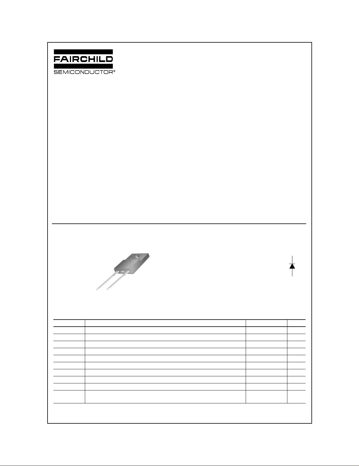
Package Symbol
TO-220F
K
A
o
C
CATHODE
Device Maximum Ratings T
Symbol Parameter Ratings Units
V
RRM
V
RWM
V
R
I
F(AV)
I
FRM
I
FSM
P
D
E
AVL
, T
T
J
STG
T
L
CAUTION: Stresses above those listed in “Device Maximum Ratings” may cause permanent damage to the device. This is a stress only rating and
operation of the device at these or any other conditions above those indicated in the operational sections of this specification is not implied.
©2003 Fairchild Semiconductor Corporation
ANODE
= 25°C unless otherwise noted
C
Peak Repetitive Reverse Voltage 600 V
Working Peak Reverse Voltage 600 V
DC Blocking Voltage 600 V
Average Rectified Forw ard Current (TC = 75oC) 8 A
Repetitive Peak Surge Current (20kHz Square Wave) 16 A
Nonrepetitive Peak Surge Current (Halfwave 1 Phase 60Hz) 100 A
Power Dissipation 26 W
Avalanche Energy (1A, 40mH) 20 mJ
Operating and Storage Temperature Range -55 to 150 °C
Maximum Temperature for Soldering
Leads at 0.063in (1.6mm) from Case for 10s 300 °C
ISL9R860PF2 Rev. A
Package Marking and Ordering Information
Device Marking Device Package Tape Width Quantity
R860PF2 ISL9R860PF2 TO-220F N/A 50 Units
ISL9R860PF2
Electrical Characteristics
TC = 25°C unless otherwise noted
Symbol Parameter Test Conditions Min Typ Max Units
Off State Characteristics
I
Instantaneous Reverse Current VR = 600V TC = 25°C - - 100 µA
R
T
= 125°C--1.0mA
C
On State Characteristics
V
Instantaneous Forward Voltage IF = 8A TC = 25°C-2.02.4V
F
= 125°C-1.62.0V
T
C
Dynamic Characteristics
C
Junction Capacitance VR = 10V, IF = 0A - 30 - pF
J
Switching Characteristics
t
Reverse Recovery Time IF = 1A, dIF/dt = 100A/µs, VR = 30V - 18 25 ns
rr
Reverse Recovery Time IF = 8A,
t
rr
I
RRM
Q
Maximum Reverse Recovery Current - 3.2 - A
Reverse Recovery Charge - 50 - nC
RR
t
Reverse Recovery Time IF = 8A,
rr
S Softness Factor (t
I
RRM
Q
Maximum Reverse Recovery Current - 3.4 - A
Reverse Recovery Charge - 150 - nC
RR
Reverse Recovery Time IF = 8A,
t
rr
S Softness Factor (t
I
Q
dI
RRM
Maximum Reverse Recovery Current - 6.5 - A
Reverse Recovery Charge 195 - nC
RR
/dt Maximum di/dt during t
M
)-3.7-
b/ta
)-2.5-
b/ta
b
= 8A, dIF/dt = 100A/µs, VR = 30V - 21 30 ns
I
F
-28-ns
/dt = 200A/µs,
dI
F
V
= 390V, TC = 25°C
R
-77-ns
/dt = 200A/µs,
dI
F
V
= 390V,
R
= 125°C
T
C
-53-ns
/dt = 600A/µs,
dI
F
V
= 390V,
R
= 125°C
T
C
- 500 - A/µs
Thermal Characteristics
R
R
©2003 Fairchild Semiconductor Corporation ISL9R860PF2 Rev. A
Thermal Resistance Junction to Case - - 4.8 °C/W
θJC
Thermal Resistance Junction to Ambient TO-220F - - 70 °C/W
θJA

Typical Performance Curves
ISL9R860PF2
16
14
12
10
8
6
, FORWARD CURRENT (A)
4
F
I
2
0
0 0.5 0.75 1 2.50.25 1.5 2 2.25
VF, FORWARD VOLTAGE (V)
175oC
150oC
125oC
25oC
100oC
1.751.25
2.75
100
10
1
, REVERSE CURRENT (µA)
R
I
0.1
100 200 300 500 600400
VR, REVERSE VOLTAGE (V)
175oC
150oC
125oC
100oC
25oC
Figure 1. Forward Current vs Forward Voltage Figure 2. Reverse Current vs Reverse Voltage
80
VR = 390V, TJ = 125°C
70
60
50
40
30
t, RECOVERY TIMES (ns)
20
10
0
0
Figure 3. t
tb AT dIF/dt = 200A/µs, 500A/µs, 800A/µs
ta AT dIF/dt = 200A/µs, 500A/µs, 800A/µs
2 4 6 8 12 14
IF, FORWARD CURRENT (A)
and tb Curves vs Forward Current Figure 4. ta and tb Curves vs dIF/dt
a
10 16
90
80
70
60
50
40
30
t, RECOVERY TIMES (ns)
20
10
0
100
VR = 390V, TJ = 125°C
tb AT IF = 16A, 8A, 4A
ta AT IF = 16A, 8A, 4A
200 300 400 500 600 800 900
dIF/dt, CURRENT RATE OF CHANGE (A/µs)
700 1000
11
VR = 390V, TJ = 125°C
10
9
8
7
6
5
4
3
, MAX REVERSE RECOVERY CURRENT (A)
RRM
2
I
0
2 4 6 8 10 12 14
IF, FORWARD CURRENT (A)
dIF/dt = 800A/µs
dIF/dt = 500A/µs
dIF/dt = 200A/µs
16
Figure 5. Maximum Reverse Recovery Current vs
Forward Current
©2003 Fairchild Semiconductor Corporation ISL9R860PF2 Rev. A
14
VR = 390V, TJ = 125°C
12
10
8
6
4
2
, MAX REVERSE RECOVERY CURRENT (A)
RRM
I
0
200 300 400 500 600 800 900
100
IF = 8A
dI
/dt, CURRENT RATE OF CHANGE (A/µs)
F
IF = 16A
IF = 4A
700 1000
Figure 6. Maximum Reverse Recovery Current vs
dI
/dt
F

Typical Performance Curves (Continued)
ISL9R860PF2
6
VR = 390V, TJ = 125°C
5
350
VR = 390V, TJ = 125°C
300
IF = 16A
250
4
IF = 16A
IF = 8A
200
IF = 8A
3
150
2
S, REVERSE RECOVERY SOFTNESS FACTOR
1
100
IF = 4A
200 300 400 500 600 800 900
700 1000
dIF/dt, CURRENT RATE OF CHANGE (A/µs)
, REVERSE RECOVERY CHARGE (nC)
100
RR
Q
50
100 700 1000200 300 400 500 600 800 900
dIF/dt, CURRENT RATE OF CHANGE (A/µs)
IF = 4A
Figure 7. Reverse Recovery Softness Factor vs dIF/dt Figure 8. Rever s e Recovery Charge vs dIF/dt
, JUNCTION CAPACITANCE (pF)
J
C
1200
1000
800
600
400
200
0
0.1 100101
VR, REVERSE VOLTAGE (V)
10
8
6
4
2
, AVERAGE FORWARD CURRENT (A)
F(AV)
0
I
T
, CASE TEMPERATURE (oC)
C
10050 150
12575
Figure 9. Junction Capacitance vs Reverse Voltage Figure 10. DC Current Derating Curve
2.0
DUTY CYCLE - DESCENDING ORDER
1.0
0.5
0.2
0.1
0.05
0.02
0.1
, NORMALIZED
Z
0.01
θJA
0.01
THERMAL IMPEDANCE
SINGLE PULSE
NOTES:
DUTY FACTOR: D = t
PEAK TJ = PDM x Z
P
DM
t
1
t
2
1/t2
x R
+ T
θJA
θJA
A
0.001
-5
10
-4
10
-3
10
-2
10
-1
10
0
10
1
10
t, RECTANGULAR PULSE DURATION (s)
Figure 11. Normalized Maximum Transient Thermal Impedance
©2003 Fairchild Semiconductor Corporation ISL9R860PF2 Rev. A

Test Circuits and Waveforms
VGE AMPLITUDE AND
RG CONTROL dIF/dt
t
AND t2 CONTROL I
1
V
GE
t
1
F
RG
t
2
L
DUT
MOSFET
CURRENT
SENSE
ISL9R860PF2
dI
F
I
F
dt
0
+
V
DD
-
t
rr
t
a
t
b
0.25 I
RM
I
RM
Figure 12. trr Test Circuit
I = 1A
L = 40mH
R < 0.1Ω
= 50V
V
DD
= 1/2LI2 [V
E
AVL
Q
= IGBT (BV
1
R(AVL)
CES
/(V
R(AVL)
> DUT V
Q1
R(AVL)
- VDD)]
)
CURRENT
SENSE
LR
DUT
Figure 14. Avalanche Energy Test Circuit
Figure 13. t
Waveforms and Definitions
rr
V
AVL
+
I
V
DD
IV
L
I
L
t
0
t
1
t
2
t
Figure 15. Avalanche Current and Voltage
Waveforms
©2003 Fairchild Semiconductor Corporation ISL9R860PF2 Rev. A

TRADEMARKS
The following are registered and unregistered trademarks Fairchild Semiconductor owns or is authorized to use and is
not intended to be an exhaustive list of all such trademarks.
ACEx
ActiveArray
Bottomless
CoolFET
CROSSVOL T
DOME
EcoSPARK
E2CMOS
EnSigna
TM
TM
FACT
FACT Quiet Series
â
FAST
FASTr
FRFET
GlobalOptoisolator
GTO
HiSeC
I2C
Across the board. Around the world.
The Power Franchise
Programmable Active Droop
ImpliedDisconnect
ISOPLANAR
LittleFET
MicroFET
MicroPak
MICROWIRE
MSX
MSXPro
OCX
OCXPro
OPTOLOGIC
â
OPTOPLANAR
PACMAN
POP
Power247
PowerTrench
â
QFET
QS
QT Optoelectronics
Quiet Series
RapidConfigure
RapidConnect
SILENT SWITCHER
SMART START
SPM
Stealth
SuperSOT-3
SuperSOT-6
SuperSOT-8
SyncFET
TinyLogic
TruTranslation
UHC
UltraFET
â
VCX
â
â
DISCLAIMER
FAIRCHILD SEMICONDUCTOR RESERVES THE RIGHT TO MAKE CHANGES WITHOUT FURTHER
NOTICE TO ANY PRODUCTS HEREIN TO IMPROVE RELIABILITY, FUNCTION OR DESIGN. FAIRCHILD
DOES NOT ASSUME ANY LIABILITY ARISING OUT OF THE APPLICATION OR USE OF ANY PRODUCT
OR CIRCUIT DESCRIBED HEREIN; NEITHER DOES IT CONVEY ANY LICENSE UNDER ITS PATENT
RIGHTS, NOR THE RIGHTS OF OTHERS.
LIFE SUPPORT POLICY
FAIRCHILDS PRODUCTS ARE NOT AUTHORIZED FOR USE AS CRITICAL COMPONENTS IN LIFE SUPPORT
DEVICES OR SYSTEMS WITHOUT THE EXPRESS WRITTEN APPROVAL OF FAIRCHILD SEMICONDUCTOR CORPORATION.
As used herein:
1. Life support devices or systems are devices or
systems which, (a) are intended for surgical implant into
the body, or (b) support or sustain life, or (c) whose
failure to perform when properly used in accordance
with instructions for use provided in the labeling, can be
reasonably expected to result in significant injury to the
user.
PRODUCT STATUS DEFINITIONS
Definition of Terms
Datasheet Identification Product Status Definition
Advance Information
Preliminary
No Identification Needed
Formative or
In Design
First Production
Full Production
2. A critical component is any component of a life
support device or system whose failure to perform can
be reasonably expected to cause the failure of the life
support device or system, or to affect its safety or
effectiveness.
This datasheet contains the design specifications for
product development. Specifications may change in
any manner without notice.
This datasheet contains preliminary data, and
supplementary data will be published at a later date.
Fairchild Semiconductor reserves the right to make
changes at any time without notice in order to improve
design.
This datasheet contains final specifications. Fairchild
Semiconductor reserves the right to make changes at
any time without notice in order to improve design.
Obsolete
Not In Production
This datasheet contains specifications on a product
that has been discontinued by Fairchild semiconductor.
The datasheet is printed for reference information only.
Rev. I2
 Loading...