ISL9R1560PF2
15A, 600V Stealth™ Diode
ISL9R1560PF2
April 2003
General Description
The ISL9R1560PF2 is a Stealth ™ diode optimized for
low loss performance in high frequency hard switched
applications. The Stealth™ family exhibits low reverse
recovery curre nt (I
recovery under typical opera tin g conditions.
This device is intended for use as a free wheeling or
boost diode in power supplies and other power
switching applications. The low I
phase reduce loss in switching tra nsistors. The soft
recovery minimizes ringin g, expandin g the range of
conditions under whic h th e diode may be operated
without the use of additional snubber circuitry . Consider
using the Stealth™ diode with an SM PS I GBT t o
provid e t he most efficient and high est power de nsity
design at lower cost.
Formerly developmental type TA49410.
) and exceptionally soft
RM(REC)
RM(REC)
and short ta
Features
• Soft Recovery. . . . . . . . . . . . . . . . . . . . . .tb / ta > 1.2
• Fast Recovery. . . . . . . . . . . . . . . . . . . . . . .t
< 30ns
rr
• Operating Temperature. . . . . . . . . . . . . . . . . . 150
• Reverse Voltage . . . . . . . . . . . . . . . . . . . . . . . . 600V
• Internally Isolated . . . . . . . . . . . . . . . . . . . . . . . . 1kV
• Avalanche Energy Rated
Applications
• Switch Mode Power Supplies
• Hard Switched PFC Boost Diod e
• UPS Free Wheeling Diode
• Motor Drive FWD
• SMPS FWD
• Snubber Diode
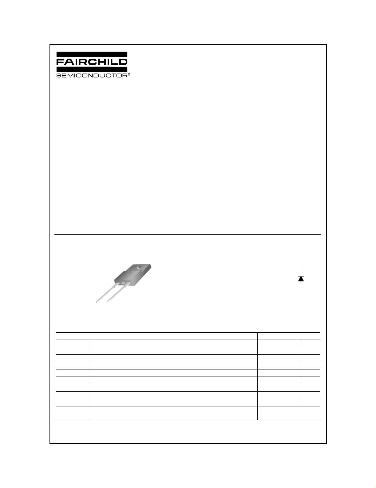
Package Symbol
TO-220F
K
A
CATHODE
ANODE
o
C
Device Maximum Ratings T
Symbol Parameter Ratings Units
V
RRM
V
RWM
V
I
F(AV)
I
FRM
I
FSM
P
E
AVL
, T
T
J
T
CAUTION: Stresses above those listed in “Device Maximum Ratings” may cause permanent damage to the device. This is a stress only rating and
operation of the device at these or any other conditions above those indicated in the operational sections of this specification is not implied.
©2003 Fairchild Semiconductor Corporation
Repetitive Peak Reverse Voltage 600 V
Working Peak Reverse Voltage 600 V
DC Blocking Voltage 600 V
R
Average Rectified Forw ard Current (TC = 25oC) 15 A
Repetitive Peak Surge Current (20kHz Square Wave) 30 A
Nonrepetitive Peak Surge Current (Halfwave 1 Phase 60Hz) 200 A
Power Dissipation 30 W
D
Avalanche Energy (1A, 40mH) 20 mJ
Operating and Storage Temperature Range -55 to 150 °C
STG
Maximum Temperature for Soldering
L
Leads at 0.063in (1.6mm) from Case for 10s 300 °C
= 25°C unless otherwise noted
C
ISL9R1560PF2 Rev. A1

Package Marking and Ordering Information
Device Marking Device Package Tape Width Quantity
R1560PF2 ISL9R1560PF2 TO-220F N/A 50
ISL9R1560PF2
Electrical Characteristics
TC = 25°C unless otherwise noted
Symbol Parameter Test Conditions Min Typ Max Units
Off State Characteristics
I
Instantaneous Reverse Current VR = 600V TC = 25°C - - 100 µA
R
= 125°C--1.0mA
T
C
On State Characteristics
V
Instantaneous Forward Voltage IF = 15A TC = 25°C-1.82.2V
F
T
= 125°C - 1.65 2.0 V
C
Dynamic Characteristics
C
Junction Capacitance VR = 10V, IF = 0A - 62 - pF
J
Switching Characteristics
t
Reverse Recovery Time IF = 1A, dIF/dt = 100A/µs, VR = 30V - 25 30 ns
rr
= 15A, dIF/dt = 100A/µs, VR = 30V - 35 40 ns
I
F
t
Reverse Recovery Time IF = 15A,
rr
I
RM(REC)
Q
Maximum Reverse Recovery Current - 3.5 - A
Reverse Recovered Charge - 57 - nC
RR
t
Reverse Recovery Time IF = 15A,
rr
S Softness Factor (t
I
RM(REC)
Q
Maximum Reverse Recovery Current - 5.0 - A
Reverse Recovered Charge - 275 - nC
RR
Reverse Recovery Time IF = 15A,
t
rr
S Softness Factor (t
I
RM(REC)
Q
dI
Maximum Reverse Recovery Current - 13.5 - A
Reverse Recovered Charge - 390 - nC
RR
/dt Maximum di/dt during t
M
/dt = 200A/µs,
dI
F
= 390V, TC = 25°C
V
R
/dt = 200A/µs,
dI
)-2.0-
b/ta
) - 1.36 -
b/ta
b
F
= 390V,
V
R
T
= 125°C
C
/dt = 800A/µs,
dI
F
= 390V,
V
R
T
= 125°C
C
- 29.4 - ns
-90-ns
-52-ns
- 800 - A/µs
Thermal Characteristics
R
R
©2003 Fairchild Semiconductor Corporation ISL9R1560PF2 Rev. A1
Thermal Resistance Junction to Case - - 4.1 °C/W
θJC
Thermal Resistance Junction to Ambient TO-247 - - 70 °C/W
θJA
 Loading...