

June 2003
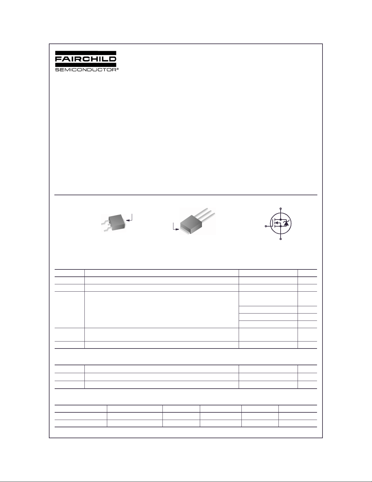
ISL9N306AD3 / ISL9N306AD3ST
N-Channel Logic Level PWM Optimized UltraFET® Trench Power MOSFETs
30V, 50A, 6mΩ
ISL9N306AD3 / ISL9N306AD3ST
General Description
This device employs a new advanced trench MOSFET
Features
•Fast switching
technology and features low gate charge while maintaining
low on-resistance.
Optim ized for swit ch ing appl icat ions , t his devi ce i mpr ove s
the overall efficiency of DC/DC converters and allows
operation to higher switching frequencies.
Applications
• DC/DC converters
DRAIN (FLANGE)
DRAIN
GATE
SOURCE
(FLANGE)
TO-252
MOSFET Maximum Ratings T
= 25°C unless otherwise noted
A
•r
•r
•Q
•Q
•C
TO-251
= 0.0052Ω (Typ), VGS = 10V
DS(ON)
= 0.0085Ω (Typ), VGS = 4.5V
DS(ON)
(Typ) = 30nC, VGS = 5V
g
(Typ) = 11nC
gd
(Typ) = 3400pF
ISS
SOURCE
DRAIN
GATE
D
G
S
Symbol Parameter Ratings Units
V
DSS
V
GS
Drain to Sou r c e Voltage 30 V
Gate to Source Voltage ±20 V
Drain Curr e nt
Continuous (T
I
D
Continuous (T
Continuous (T
= 25oC, VGS = 10V)
C
= 100oC, VGS = 4.5V) 50 A
C
= 25oC, VGS = V, R
C
= 52oC/W) 16 A
θJC
50 A
Pulsed Figure 4 A
P
D
T
, T
J
STG
Power dissipation
Derate above 25
o
C
Operating and Storage Temperature -55 to 175
125
0.83
W
W/oC
o
C
Thermal Characteristics
R
θJC
R
θJA
R
θJA
Thermal Resistance Junction to Case TO-251, TO-252 1.2
Thermal Resistance Junction to Ambient TO-251, TO-252 100
Thermal Resistance Junction to Ambient TO-252, 1in2 copper pad ar ea 52
Package Marking and Ordering Information
Device Marking Device Package Reel Size Tape Width Quantity
N306AD ISL9N306AD3ST TO-252AA 330mm 16mm 2500 units
N306AD ISL9N306AD3 TO-25 1AA Tube N/A 75 unit s
©2003 Fairchild Semiconductor Corporation
ISL9N 306AD3 / ISL9N306AD3ST Rev. B2
o
C/W
o
C/W
o
C/W
ISL9N306AD3 / ISL9N306AD3ST
Electrical Characteristics T
= 25°C unless otherwise noted
A
Symbol Parameter Test Conditions Min Typ Max Units
Off Characteristics
B
I
DSS
I
GSS
VDSS
Drain to Sou r c e Br ea kd ow n Voltage ID = 250µA, VGS = 0V 30 - - V
V
= 25V - - 1
Zero Gate Voltage Drain Current
DS
= 0V TC = 150
V
GS
o
--250
Gate to Source Leakage Current VGS = ±20V - - ±100 nA
On Characteristics
V
GS(TH)
r
DS(ON)
Gate to Source Threshold Voltage VGS = VDS, ID = 250µA1-3V
I
= 50A, VGS = 10V - 0.0052 0.0060
Drain to S ou r c e On Re si st ance
D
= 50A, VGS = 4.5V - 0.0085 0.0095
I
D
Dynamic Characteristics
C
C
C
Q
Q
Q
Q
Q
ISS
OSS
RSS
g(TOT)
g(5)
g(TH)
gs
gd
Input Capacitance
Output Capacitance - 650 - pF
Reverse Transfer Capacitance - 300 - pF
Total Gate Charge at 10V VGS = 0V to 10V
Total Gate Charge at 5V VGS = 0V to 5V - 30 45 nC
Threshold Gate Charge VGS = 0V to 1V - 3.0 4.5 nC
Gate to Source Gate Charg e - 10 - n C
Gate to Drain “Miller” Charge - 11 - nC
Switching Characteristics
t
ON
t
d(ON)
t
r
t
d(OFF)
t
f
t
OFF
Turn-On Time
Turn-On Delay Time - 16 - ns
Rise Time - 70 - ns
Turn-Off Delay Time - 34 - ns
Fall Time - 30 - ns
Turn-Off T ime - - 97 ns
(VGS = 4.5V)
= 15V, VGS = 0V,
V
DS
f = 1MHz
V
= 15V, ID = 16A
DD
V
= 4.5V, RGS = 4.3Ω
GS
= 15V
V
DD
I
= 50A
D
I
= 1.0mA
g
-3400- pF
-6090nC
--131ns
µA
Ω
Switching Characteristics (V
t
ON
t
d(ON)
t
r
t
d(OFF)
t
f
t
OFF
Turn-On Time
Turn-On Delay Time - 10 - ns
Rise Time - 43 - ns
Turn-Off Delay Time - 62 - ns
Fall Time - 29 - ns
Turn-Off T ime - - 137 ns
GS
= 10V)
V
= 15V, ID = 16A
DD
V
= 10V, RGS = 4.3Ω
GS
- - 80 ns
Unclamped Inductive Switching
t
AV
Avalanche Tim e ID = 30A, L = 200µH428--µs
Drain-Source Diode Characteristics
I
= 50A - - 1.25 V
V
SD
t
rr
Q
RR
©2003 Fairchild Semiconductor Corporation ISL9N 306AD3 / ISL9N306AD3ST Rev. B2
Source to Drain Diode Voltage
Reverse Recovery Time ISD = 50A, dISD/dt = 100A/µs- - 35 ns
Reverse Recovered Charge ISD = 50A, dISD/dt = 100A/µs- - 30 nC
SD
= 25A - - 1.0 V
I
SD
Typical Cha racteristic
ISL9N306AD3 / ISL9N306AD3ST
1.2
1.0
0.8
0.6
0.4
0.2
POWER DISSIPATION MULTIPLIER
0
0 25 50 75 100 175
125
150
TC, CASE TEMPERATURE (oC)
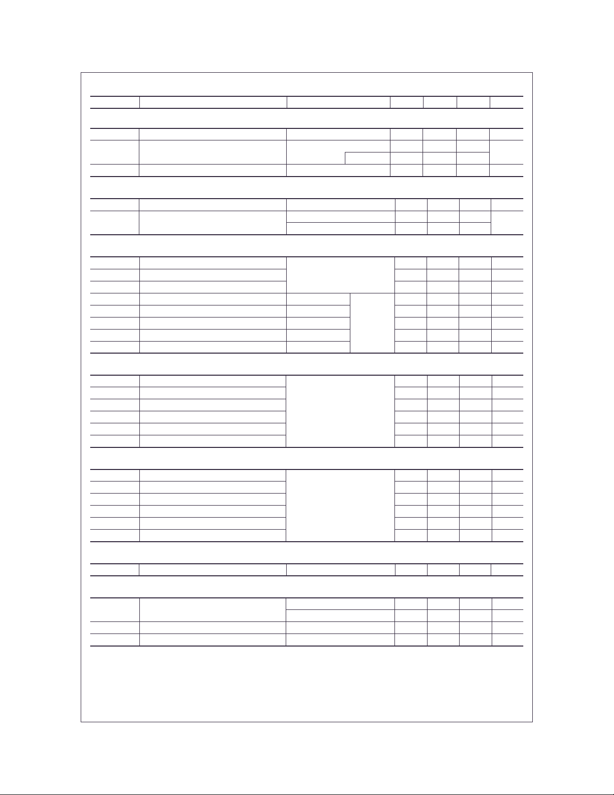
Figure 1. Normalized Power Dissipation vs
Ambient Temperature
2
DUTY CYCLE - DESCENDING ORDER
0.5
1
0.2
0.1
0.05
0.02
0.01
0.1
, NORMALIZED
θJC
Z
THERMAL IMPEDANCE
0.01
-5
10
-4
10
SINGLE PULSE
-3
10
t, RECTANGULAR PULSE DURATION (s)
60
50
VGS = 10V
40
VGS = 4.5V
30
20
, DRAIN CURRENT (A)
D
I
10
0
25 50 75 100 125 150 175
TC, CASE TEMPERATURE (oC)
Figure 2. Maximum Continuous Drain Curr ent vs
Case Temperature
P
DM
t
1
t
0
x R
θJC
+ T
2
C
1
10
NOTES:
DUTY FACTOR: D = t
PEAK TJ = PDM x Z
-2
10
-1
10
1/t2
θJC
10
Figure 3. Normalize d Maxim um transient Thermal Impedance
2000
1000
, PEAK CURRENT (A)
DM
I
100
TRANSCONDUCTANCE
MAY LIMIT CURRENT
IN THIS REGION
40
-5
10
VGS = 10V
VGS = 5V
-4
10
-3
10
-2
10
-1
10
t, PULSE WIDTH (s)
TC = 25oC
FOR TEMPERATURES
o
ABOVE 25
CURRENT AS FOLLOWS:
I = I
25
C DERATE PEAK
175 – T
150
0
10
C
1
10
Figure 4. Peak Current Capability
©2003 Fairchild Semiconductor Corporation ISL9N 306AD3 / ISL9N306AD3ST Rev. B2
Typical Cha racteristic (Conti nued)
ISL9N306AD3 / ISL9N306AD3ST
100
PULSE DURATION = 80µs
DUTY CYCLE = 0.5% MAX
V
= 15V
DD
75
50
, DRAIN CURRENT (A)
25
D
I
TJ = 25oC
0
12345
TJ = 175oC
TJ = -55oC
VGS, GATE TO SOURCE VOLTAGE (V)
100
VGS = 10V
75
50
, DRAIN CURRENT (A)
25
D
I
0
0 0.5 1.0 1.5 2.0
VDS, DRAIN TO SOURCE VOLTAGE (V)
VGS = 4.5V
T
PULSE DURATION = 80µs
DUTY CYCLE = 0.5% MAX
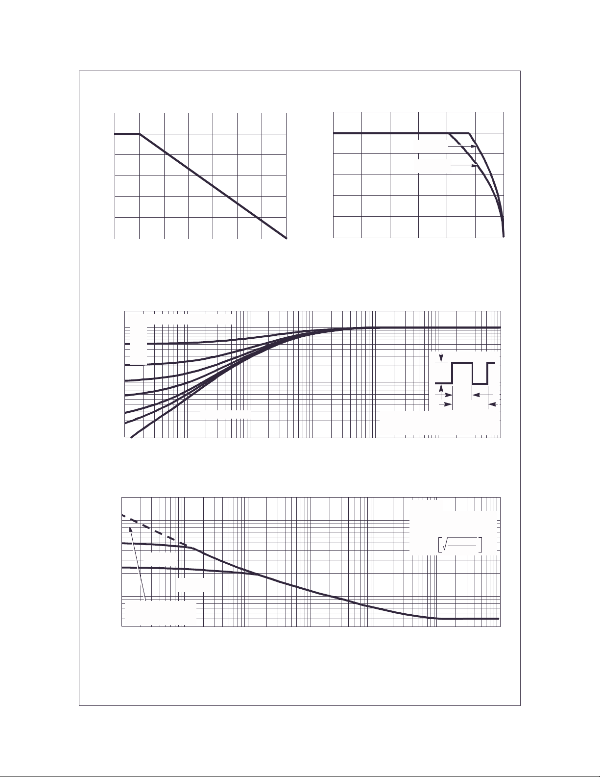
Figure 5. Transfer Characteristics Figure 6. Saturation Characteristics
25
20
15
, DRAIN TO SOURCE
DS(ON)
r
ID =5A
ON RESISTANCE (mΩ)
10
5
246810
ID = 25A
ID = 50A
V
, GATE TO SOURCE VOLTAGE (V)
GS
PULSE DURATION = 80µs
DUTY CYCLE = 0.5% MAX
T
= 25oC
C
2.0
PULSE DURATION = 80µs
DUTY CYCLE = 0.5% MAX
1.5
ON RESISTANCE
1.0
NORMALIZED DRAIN TO SOURCE
0.5
-80 -40 0 40 80 120 160 200
TJ, JUNCTION TEMPERATURE (oC)
= 25oC
C
VGS = 10V, ID = 50A
VGS = 3.5V
VGS = 3V
Figure 7. Drain to Source O n Resistance vs Gate
Voltage and Drain Current
1.4
1.0
0.6
NORMALIZED GATE
THRESHOLD VOLTAGE
0.2
-80 -40 0 40 80 120 160 200
TJ, JUNCTION TEMPERATURE (oC)
VGS = VDS, ID = 250µA
Figure 9. Normali zed Gate Threshold Voltage vs
Junction Temperatur e
©2003 Fairchild Semiconductor Corporation ISL9N 306AD3 / ISL9N306AD3ST Rev. B2
Figure 8. Normalized Drain to Source On
Resistance vs Junction Temperature
1.2
1.1
1.0
BREAKDOWN VOLTAGE
NORMALIZED DRAIN TO SOURCE
0.9
-80 -40 0 40 80 120 160 200
T
, JUNCTION TEMPERATURE (oC)
J
ID = 250µA
Figure 10. Normalized Drain to Source
Breakdown Voltage vs Junction Temperature

Typical Cha racteristic (Conti nued)
ISL9N306AD3 / ISL9N306AD3ST
5000
C
= CGS + C
ISS
GD
C
≅ C
OSS
DS
1000
C
= C
RSS
GD
C, CAPACITANCE (pF)
V
= 0V, f = 1MHz
GS
100
0.1 1 10
VDS, DRAIN TO SOURCE VOLTAGE (V)
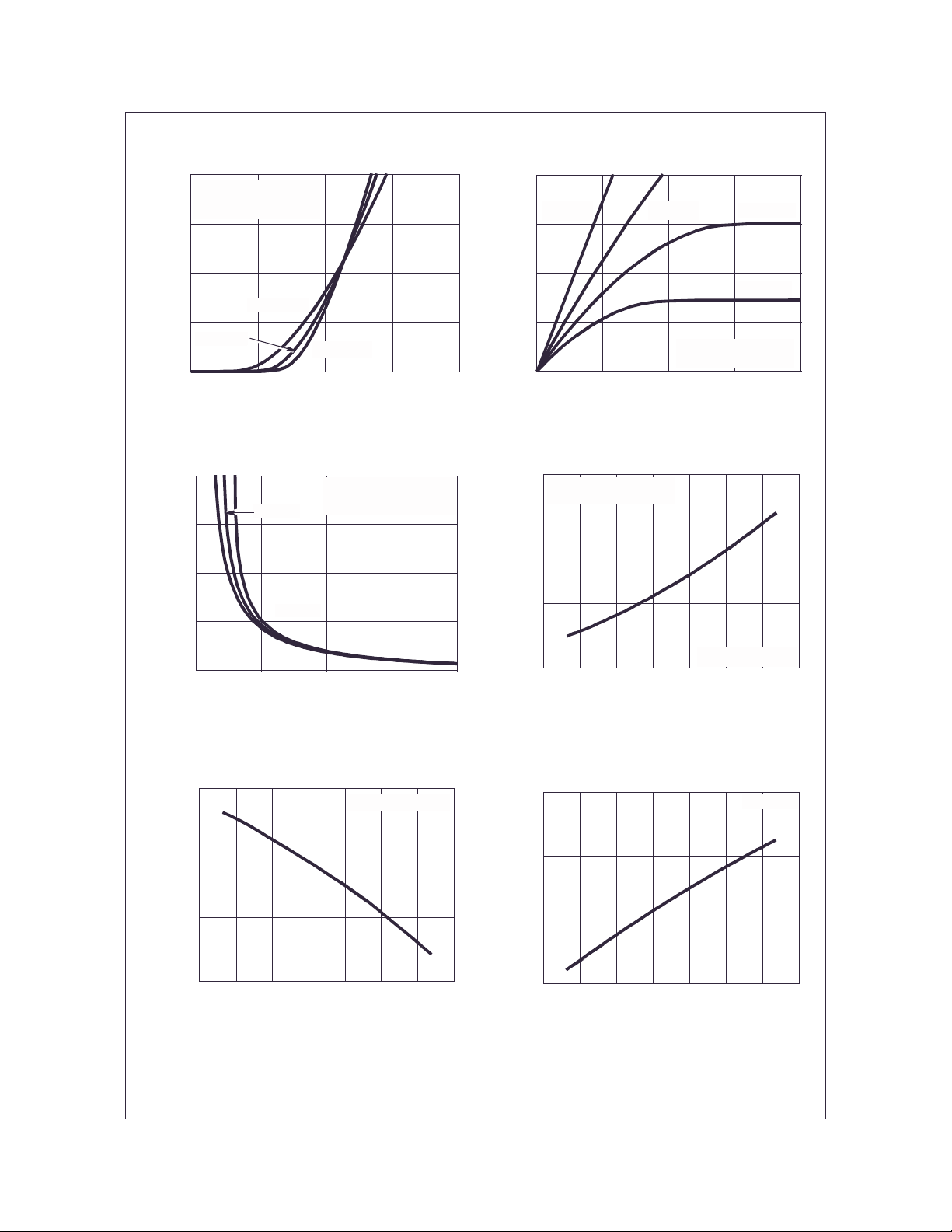
Figure 11. Capacitance vs Drain to Sour ce
Voltage
300
VGS = 4.5V, VDD = 15V, ID = 16A
250
200
t
150
100
SWITCHING TIME (ns)
50
0
0 1020304050
RGS, GATE TO SOURCE RESISTANCE (Ω)
r
t
d(ON)
t
d(OFF)
+ C
10
VDD = 15V
8
GD
6
4
WAVEFORMS IN
2
, GATE TO SOURCE VOLTAGE (V)
GS
0
V
30
0102030 405060
DESCENDING ORDER:
ID = 50A
I
= 25A
D
I
= 5A
D
Qg, GATE CHARGE (nC)
Figure 12. Gat e Charge Waveforms for Constant
Gate Currents
500
VGS = 10V, VDD = 15V, ID = 16A
400
t
f
300
t
d(OFF)
200
t
SWITCHING TIME (ns)
100
f
t
r
0
0 1020304050
RGS, GATE TO SOURCE RESISTANCE (Ω)
t
d(ON)
Figure 13. Switching Time vs Gate Resist ance Figure 14. Switching Time vs Gate Resistance
Test Circuits and Waveforms
V
DS
L
I
TO OBTAIN
VARY t
P
REQUIRED PEAK I
V
GS
R
AS
G
+
V
DD
-
AS
DUT
t
0V
P
I
AS
0
0.01Ω
Figure 15. Unclamped Energy Test Circuit Figure 16. Unclamped Energy Waveforms
©2003 Fairchild Semiconductor Corporation ISL9N 306AD3 / ISL9N306AD3ST Rev. B2
BV
DSS
t
P
t
AV
V
DS
V
DD

Test Circuits and Waveforms (Cont i nu ed )
V
DS
R
L
V
GS
+
V
DD
-
DUT
I
g(REF)
Figure 17. Gate Charge Test Circuit Figure 18. Gate Charge Waveforms
V
DD
V
0
I
g(REF)
0
GS
V
= 1V
Q
g(TOT)
V
DS
Q
g(5)
GS
Q
g(TH)
Q
gs
Q
gd
VGS = 5V
ISL9N306AD3 / ISL9N306AD3ST
V
= 10V
GS
V
DS
R
L
V
GS
R
GS
V
GS
DUT
+
V
DD
-
V
DS
0
V
GS
10%
0
t
d(ON)
90%
t
ON
t
r
10%
PULSE WIDTH
Figure 19. Switching Time Test Circuit Figure 20. Switching Time Waveforms
t
d(OFF)
90%
t
OFF
t
f
90%
10%
50%50%
©2003 Fairchild Semiconductor Corporation ISL9N 306AD3 / ISL9N306AD3ST Rev. B2

Thermal Resistance vs. Mounting Pad Area
125
The maximum rated junction temperature, TJM, and the
thermal resistance of the heat dissipating path determines
the maxi mum al lowab le de vice p ower di ssip ation, P
application. Therefore the application’s ambient
temperature, T
must be reviewed to ensure that T
Equation 1 mathematically represents the relationship and
(oC), and th ermal res istance R
A
is never exceeded.
JM
serve s as the basis for establ ishing the rating of the part.
TJMTA–()
P
----------------- ------------=
DM
Z
θJA
DM
(oC/W)
θJA
(EQ. 1)
, in an
100
C/W)
o
(
θJA
R
ISL9N306AD3 / ISL9N306AD3ST
R
= 33.32 + 23.84/(0.268+Area)
θJA
75
50
In using surface mount devices such as the TO-252
package, the environment in which it is applied will have a
significant influence on the part’s current and maximum
power d issipati on rating s. Precise d etermin ation of P
comple x and influenced by many factors:
DM
is
1. Mou nting pad area ont o which the device is attached and
whet her the re is copp er on one s ide or both side s of the
board.
2. The number of copper layers and the thickness of the
board.
3. The use of external heat sinks.
4. The use of thermal vias.
5. Air flow and board orientation.
6. For no n steady state applic ations, th e pulse widt h, the
duty cycle and the transient thermal response of the part,
the boa rd and the environment they are in.
Fairchild provides thermal information to assist the
designer’s preliminary application evaluation. Figure 21
defines the R
copper (component side) area. This is for a horizontally
for the device as a function of the top
θJA
positi on ed FR-4 bo ar d with 1 oz c o pp er af t er 1000 se c on ds
of stea dy st ate pow er w ith n o air flow . Th is gr aph prov ides
the necessary inf ormation for calculation of the steady state
junction temperature or power dissipation. Pulse
applications can be evaluated using the Fairchild device
Spice t hermal model or manu ally utilizin g the normal ized
maximum transient thermal impedance curve.
25
0.01 0.1 1 10
AREA, TOP COPPER AREA (in2)
Figure 21. Thermal Resistance vs Mounting
Pad Area
Displayed on the curve are R
Electrical Specifications table. The points were chosen to
values listed in the
θJA
depict the compromise between the copper board area, the
thermal resistance and ultimately the power dissipation,
P
.
DM
Therma l resi stances correspondi ng to other copper are as
can be obtained from Figure 21 or by calculation using
Equation 2. R
times a coefficient added to a constant. The area, in square
is defined as the natural log of the area
θJA
inches is the top copp er area incl uding the gate and source
pads.
θJA
33.32
R
©2003 Fairchild Semiconductor Corporation ISL9N 306AD3 / ISL9N306AD3ST Rev. B2
23.84
-------------------------------------+=
0.268 Area+()
(EQ. 2)

PSPICE Electrical Model
.SUB CK T IS L 9N306A 2 1 3 ; rev May 2001
CA 12 8 2.0e -9
CB 15 14 2.3e-9
CIN 6 8 3e-9
DBODY 7 5 DBODYMO D
DBREAK 5 11 DBREAKMOD
DPLCAP 10 5 DPLCAPMOD
EBREAK 11 7 17 18 35.8
EDS 14 8 5 8 1
EGS 13 8 6 8 1
ESG 6 10 6 8 1
EVTHRES 6 21 19 8 1
EVTEMP 20 6 18 22 1
IT 8 17 1
LDRAIN 2 5 1.0e-9
LGATE 1 9 4.58e- 9
LSOURCE 3 7 1.47e-9
MMED 16 6 8 8 MMEDM OD
MSTR O 16 6 8 8 M S T ROMOD
MWEAK 16 21 8 8 MWE AKMOD
RBREAK 17 18 RBREAKMOD 1
RDRAIN 50 16 RDRAINMOD 1e-3
RGAT E 9 20 2.69
RLDRAIN 2 5 10
RLGATE 1 9 45.8
RLSOUR CE 3 7 1 4.7
RSLC1 5 51 RSL CM OD 1e-6
RSLC2 5 50 1e3
RSOURCE 8 7 RSOURCEMOD 3.5e-3
RVTHRES 22 8 RVTHRESM OD 1
RVTEMP 18 19 RVTEMPMOD 1
GATE
1
LGATE
RLGATE
RGATE
9
CA
-
ESG
+
EVTEMP
+
-
18
22
20
S1A
12
13
8
S1B
EGS EDS
6
8
13
10
RSLC2
6
S2A
14
13
S2B
+
+
6
8
-
-
DPLCAP
EVTHRES
+
19
8
CIN
15
CB
-
+
51
5
8
-
5
RSLC1
51
+
5
50
RDRAIN
21
MSTRO
14
ESLC
16
8
MMED
8
DBREAK
11
+
17
EBREAK
18
-
MWEAK
RSOURCE
RBREAK
17 18
IT
RVTHRES
7
RLSOURCE
RVTEMP
19
-
+
22
LDRAIN
RLDRAIN
DBODY
LSOURCE
VBAT
DRAIN
2
SOURCE
3
ISL9N306AD3 / ISL9N306AD3ST
S1A 6 12 13 8 S1AMOD
S1B 13 12 13 8 S1BMOD
S2A 6 15 14 13 S2AMOD
S2B 13 15 14 13 S2BMOD
VBAT 22 19 DC 1
ESLC 51 50 VALUE={(V(5,51)/ABS(V(5,51)))*(PWR(V(5,51)/(1e-6*275),5))}
.MODEL DBODYMOD D (IS = 3.6e-11 N=1.075 RS = 3.5e-3 TRS1 = 1e-3 TRS2 = 1e-6 XTI=1.0 CJO = 1.45e-9 TT = 8e-11 M =
0.51)
.MODEL DBR EAKMOD D (RS = 1.7e-1 TRS 1 = 1e-3 TRS 2 = -8.9e-6)
.MODEL DPLC APMOD D (CJO = 11.5e-10 IS = 1e-30 N = 10 M = 0.46)
.MOD E L MM EDMOD NMO S ( VT O = 1.7 KP = 9 IS= 1e-30 N = 10 TO X = 1 L = 1u W = 1u RG = 2.69)
.MODEL MSTROM OD NMOS (VTO = 2.1 KP = 100 IS = 1e-30 N= 10 TOX = 1 L = 1u W = 1u)
.MODEL MWEAKMOD NMOS (VTO = 1.36 KP = 0.05 IS = 1e-30 N = 10 TOX = 1 L = 1u W = 1u RG = 26.9 RS = 0.1)
.MODEL RBREAKMOD RES (TC1 = 1e-3 TC2 = -7e-7)
.MODEL RD RAINMOD RES (TC1 = 1.2e-2 TC 2 = 3 .0e-5)
.MODEL RSLC M OD RES (TC1 = 1e-3 TC2 = 1e-6)
.MODEL RSOURCEMOD RES (TC1 = 1e-3 TC2 = 1e-6)
.MODEL RVTHRESMOD RES (TC1 = -2.6e-3 TC2 = -7.5e-6)
.MODEL RVT EMPMOD RES (T C1 = -1.8e-3 TC2 = 1e -6)
.MODEL S1AMOD VSWITCH (RON = 1e-5 ROFF = 0.1 VON = -4.0 VOFF= -0.8)
.MODEL S1BMOD VSWITCH (RON = 1e-5 ROFF = 0.1 VON = -0.8 VOFF= -4.0)
.MODEL S2AMOD VSWITCH (RON = 1e-5 ROFF = 0.1 VON = -0.3 VOFF= 0.2)
.MODEL S2BMOD VSWITCH (RON = 1e-5 ROFF = 0.1 VON = 0.2 VOFF= -0.3)
.ENDS
NOTE: For further discussion of the PSPICE model, con sult A New PSPICE Sub-Cir cuit for the P ower MOSFE T Featuring Global
Temperature Options; IEEE Power Electronics Specialist Conference Records, 1991, written by William J. Hepp and C. Frank
Wheatley.
©2003 Fairchild Semiconductor Corporation ISL9N 306AD3 / ISL9N306AD3ST Rev. B2

SABER Electrical Model
REV May 2001
template I SL 9N306A n2,n1,n3
electrical n2,n1,n3
{
var i iscl
dp..model dbodymod = (isl = 3.6e-11, nl=1.075 , rs = 3.5e-3, trs1 = 1e-3, tr s2 = 1e-6, xti=1.0, cjo = 1.45e-9, tt = 8e-11, m = 0.51,)
dp..model dbreakmod = (rs =0.17, trs1 = 1e-3, trs2 = -8. 9e-6)
dp..model dpl ca pm od = (cjo = 11.5e-10, isl=10e-30, nl=10 , m=0.46)
m..model mme dm od = (type=_n, vto = 1. 7, kp=9, is=1e-30, tox=1)
m..model mst rongmod = (type=_n, vto = 2.1, kp = 100, is = 1e-30, tox = 1)
m..model mweakmod = (type=_n, vto = 1.36, kp = 0.05, is = 1e-30, tox = 1, rs=0.1)
sw_vcsp..model s1amod = (ron = 1e-5, roff = 0.1, von = -4.0, voff = -0.8)
sw_vcsp.. mo del s1bmod = (ron =1e-5 , ro ff = 0.1 , v on = -0.8, voff = -4.0)
sw_vcsp.. mo del s 2am od = (ron = 1e-5, roff = 0.1, von = -0.3, voff = 0.2)
sw_vcsp.. mo del s 2bm od = (ron = 1e-5, roff = 0.1, von = 0.2, voff = -0.3)
c.ca n12 n8 = 2.0e -9
10
c.cb n15 n14 = 2.3e-9
c.cin n6 n8 = 3e-9
dp.dbody n7 n5 = model=dbodymod
dp.dbreak n5 n11 = model=dbreakmod
dp.dplcap n10 n5 = model=dplca pm od
i.it n8 n17 = 1
l.ldrain n2 n5 = 1e-9
l.lgate n1 n9 = 4.58e-9
l.lsource n3 n7 = 1.47e-9
GATE
1
LGATE
RLGATE
RGATE
9
ESG
EVTEMP
+
18
22
20
6
8
+
-
m.mmed n16 n6 n8 n8 = m odel=mmedm od, l= 1u, w=1u
m.mstrong n16 n6 n8 n8 = model=ms trongmod, l=1u, w=1u
m.mweak n16 n21 n8 n8 = model=mweakm od, l=1u, w=1u
res.rbreak n17 n18 = 1, tc1 = 1e-3, tc2 = -7 e-7
res.rdrain n50 n16 = 1e-3, tc1 = 1.2e-2, tc2 = 3.0e-5
res.rgate n9 n20 = 2.69
res.rldrai n n2 n5 = 10
res.rlgate n1 n9 = 45.8
res.rlsource n3 n7 = 14.7
res.rslc1 n5 n51= 1e-6, tc1 = 1e -3, tc 2 =1e-6
res.rslc2 n5 n50 = 1e3
12
CA
S1A
13
8
S1B
13
+
+
EGS EDS
res.rsour ce n8 n7 = 3.5e-3, tc1 = 1e-3, tc 2 =1e-6
res.rvtemp n18 n19 = 1, tc1 = -1.8e-3, tc2 = 1e-6
res.rvthres n22 n8 = 1, tc1 = -2.6e-3, tc 2 = -7.5e-6
spe.ebreak n11 n7 n17 n18 = 35.8
spe.eds n14 n8 n5 n8 = 1
spe.egs n13 n8 n6 n8 = 1
spe.esg n6 n10 n6 n8 = 1
spe.evtemp n20 n6 n18 n22 = 1
spe.evthres n6 n21 n19 n8 = 1
DPLCAP
RSLC2
EVTHRES
6
S2A
14
13
S2B
6
8
-
-
5
RSLC1
51
ISCL
16
8
MMED
8
DBREAK
11
MWEAK
EBREAK
RSOURCE
RBREAK
17 18
IT
RVTHRES
50
RDRAIN
+
21
-
19
8
MSTRO
CIN
15
CB
14
+
5
8
-
+
-
17
18
7
RLSOURCE
RVTEMP
19
-
+
22
LDRAIN
RLDRAIN
DBODY
LSOURCE
VBAT
DRAIN
2
SOURCE
3
ISL9N306AD3 / ISL9N306AD3ST
sw_vcsp.s1 a n6 n12 n13 n8 = model= s1amod
sw_vcsp.s1 b n13 n12 n13 n8 = model =s1bmod
sw_vcsp.s2 a n6 n15 n14 n13 = model =s2amod
sw_vcsp.s2 b n13 n15 n14 n13 = model =s2bmod
v.vbat n22 n19 = dc=1
equations {
i (n51->n50) +=iscl
iscl: v(n51,n50) = ((v(n5, n51)/(1e-9+abs(v(n5,n51))))*((abs(v(n5,n51)*1e-6/275))** 5))
}
}
©2003 Fairchild Semiconductor Corporation ISL9N 306AD3 / ISL9N306AD3ST Rev. B2

ISL9N306AD3 / ISL9N306AD3ST
SPICE Thermal Model
REV May 2001
ISL9N306AT
CTHERM1 t h 6 2.7e-4
CTHERM2 6 5 3. 9e-3
CTHERM3 5 4 4. 2e-3
CTHERM4 4 3 4. 8e-3
CTHERM5 3 2 1. 9e-2
CTHERM6 2 t l 5 .9e-2
RTHERM1 t h 6 1.0e-3
RTHERM2 6 5 4. 8e-3
RTHERM3 5 4 4. 5e-2
RTHERM4 4 3 2. 6e-1
RTHERM5 3 2 3. 1e-1
RTHERM6 2 t l 3 .4e-1
SABER Thermal Model
SABER therm al m odel ISL9N306AT
template thermal_model th tl
thermal_ c th , tl
{
ctherm.ctherm1 t h 6 = 2.7e-4
ctherm.ctherm2 6 5 = 3.9e-3
ctherm.ctherm3 5 4 = 4.2e-3
ctherm.ctherm4 4 3 = 4.8e-3
ctherm.ctherm5 3 2 = 1.9e-2
ctherm.cth erm6 2 tl = 5.9e-2
rtherm.rtherm1 th 6 = 1.0e-3
rtherm.rt herm2 6 5 = 4.8e-3
rtherm.rt herm3 5 4 = 4.5e-2
rtherm.rt herm4 4 3 = 2.6e-1
rtherm.rt herm5 3 2 = 3.1e-1
rtherm.rt he rm6 2 tl = 3.4e-1
}
RTHERM1
RTHERM2
RTHERM3
RTHERM4
RTHERM5
JUNCTION
th
CTHERM1
6
CTHERM2
5
CTHERM3
4
CTHERM4
3
CTHERM5
2
RTHERM6
tl
©2003 Fairchild Semiconductor Corporation ISL9N 306AD3 / ISL9N306AD3ST Rev. B2
CTHERM6
CASE

TRADEMARKS
The following are registe red and unr egistered trademarks Fairchild Semiconductor owns or is aut horized to use and is not
intended to be an exhaustive list of all such trademarks.
ACEx™
ActiveArray™
Bottomless™
CoolFET™
CROSSVOLT™
DOME™
EcoSPARK™
2
E
CMOS™
EnSigna™
Across the board. Around the world.™
The Power Fr anchise™
Programma ble Active Droop™
FACT™
FACT Quiet Series™
®
FAST
FASTr™
FRFET™
GlobalOptoisolator™
GTO™
HiSeC™
2
I
C™
ImpliedDisconnect™
ISOPLANAR™
LittleFET™
MicroFET™
MicroPak™
MICROWIRE™
MSX™
MSXPro™
OCX™
OCXPro™
OPTOLOGIC
®
OPTOPLANAR™
PACMAN™
POP™
Power247™
PowerTrench
®
QFET™
QS™
QT Optoelectronics™
Quiet Ser ies™
RapidConfigure™
RapidConnect™
SILENT SWITCHER
SMART START™
SPM™
Stealth™
SuperSOT™-3
SuperSOT™-6
SuperSOT™-8
SyncFET™
TinyLogic
TruTranslation™
UHC™
UltraFET
®
VCX™
®
®
DISCLAIMER
FAIRCHILD SEMICONDUCTOR RESERVES THE RIGHT TO MAKE CHANGES WITHOUT FURTHER NOTICE TO ANY
PRODUCTS HEREIN TO IMPROVE RELIABILITY, FUNCTION OR DESIGN. FAIRCHILD DOES NOT ASSUME ANY
LIABILITY ARISING OUT OF THE APPLICATION OR USE OF ANY PRODUCT OR CIRCUIT DESCRIBED HEREIN;
NEITHER DOES IT CONVEY ANY LICENSE UNDER ITS PATENT RIGHTS, NOR THE RIGHTS OF OTHERS.
LIFE SUPPORT POLICY
FAIRCHILD’S PRODUCTS ARE NOT AUTHORIZED FOR USE AS CRITICAL COMPONENTS IN LIFE SUPPORT
DEVICES OR SYSTEMS WITHOUT THE EXPRESS WRITTEN APPROVAL OF FAIRCHILD SEMICONDUCTOR
CORPORATION.
As used herein:
1. Life support devices or systems are devices or systems
which, (a) ar e int ende d fo r s urgic al i mpla nt into the bo dy,
or (b) support or sustain life, or (c) whose failure to perform
when properly used in accordance with instructions for use
provided in the labeling, can be reasonably expected to
result in significant injury to the user.
2. A c r it ic al c om ponent i s an y c om ponent o f a life s u pp or t
device or system whose failure to perform can be
reasonably expected to cause the failure of the life support
device or system, or to affect its safety or effectiveness.
PRODUCT STATUS DEFINITIONS
Definition of Terms
Datasheet Identification Product Status Definition
Adva nce Information Formative or I n
Design
Preliminary First Production This datasheet contains preliminary data, and
No Identification Needed Full Production This datasheet contains final specifications. Fairchild
Obsolete Not In Production This datasheet contains specifications on a prod uct
This datasheet contains the design specifications for
product development. Specifications may change in
any manner without notice.
supple m entary data will be published at a later date.
Fairchild Semiconductor reserves the right to make
changes at any time without notice in order to improve
design.
Semiconductor reserves the righ t to make chan ges at
any time without notice in order to improve design.
that has been discontinued by Fairchild semiconductor.
The datasheet is printed for reference information only.
Rev. I2

 Loading...