

Page 1
©2005 Fairchild Semiconductor Corporation
www.fairchildsemi.com
Rev.1.0.5
FPSTM is a trademark of Fairchild Semiconductor Corporation.
Features
• Internal Avalanche Rugged Sense FET
• Consumes only 0.65W at 240VAC & 0.3W load with
Advanced Burst-Mode Operation
• Frequency Modulation for EMI Reduction
• Precision Fixed Operating Frequency
• Internal Start-up Circuit
• Pulse-by-Pulse Current Limiting
• Abnormal Over Current Protection (AOCP)
• Over Voltage Protection (OVP)
• Over Load Protection (OLP)
• Internal Thermal Shutdown Function (TSD)
• Auto-Restart Mode
• Under Voltage Lockout (UVLO)
• Low Operating Current (max 3mA)
• Adjustable Peak Current Limit
• Built-in Soft Start
Applications
• SMPS for STB, Low cost DVD Player
• Auxiliary Power for PC
• Adapter & Charger
Related Application Notes
• AN-4137, 4141, 4147(Flyback) / AN-4134(Forward)
Description
Each product in the FSDx321 (x for H, L) family consists of
an integrated Pulse Width Modulator (PWM) and Sense
FET, and is specifically designed for high performance offline Switch Mode Power Supplies (SMPS) with minimal
external components. Both devices are integrated high voltage power switching regulators which combine an avalanche
rugged Sense FET with a current mode PWM control block.
The integrated PWM controller features include: a fixed
oscillator with frequency modulation for reduced EMI,
Under Voltage Lock Out (UVLO) protection, Leading Edge
Blanking (LEB), an optimized gate turn-on/turn-off driver,
Thermal Shut Down (TSD) protection, Abnormal Over Current Protection (AOCP) and temperature compensated precision current sources for loop compensation and fault
protection circuitry. When compared to a discrete MOSFET
and controller or RCC switching converter solution, the
FSDx321 devices reduce total component count, design size,
weight while increasing efficiency, productivity and system
reliability. Both devices provide a basic platform that is well
suited for the design of cost-effective flyback converters.
Notes:
1. Typical continuous power in a non-ventilated enclosed
adapter with sufficient drain pattern as a heat sinker, at
50°C ambient.
2. Maximum practical continuous power in an open frame
design with sufficient drain pattern as a heat sinker, at 50°C
ambient.
3. 230 VAC or 100/115 VAC with doubler.
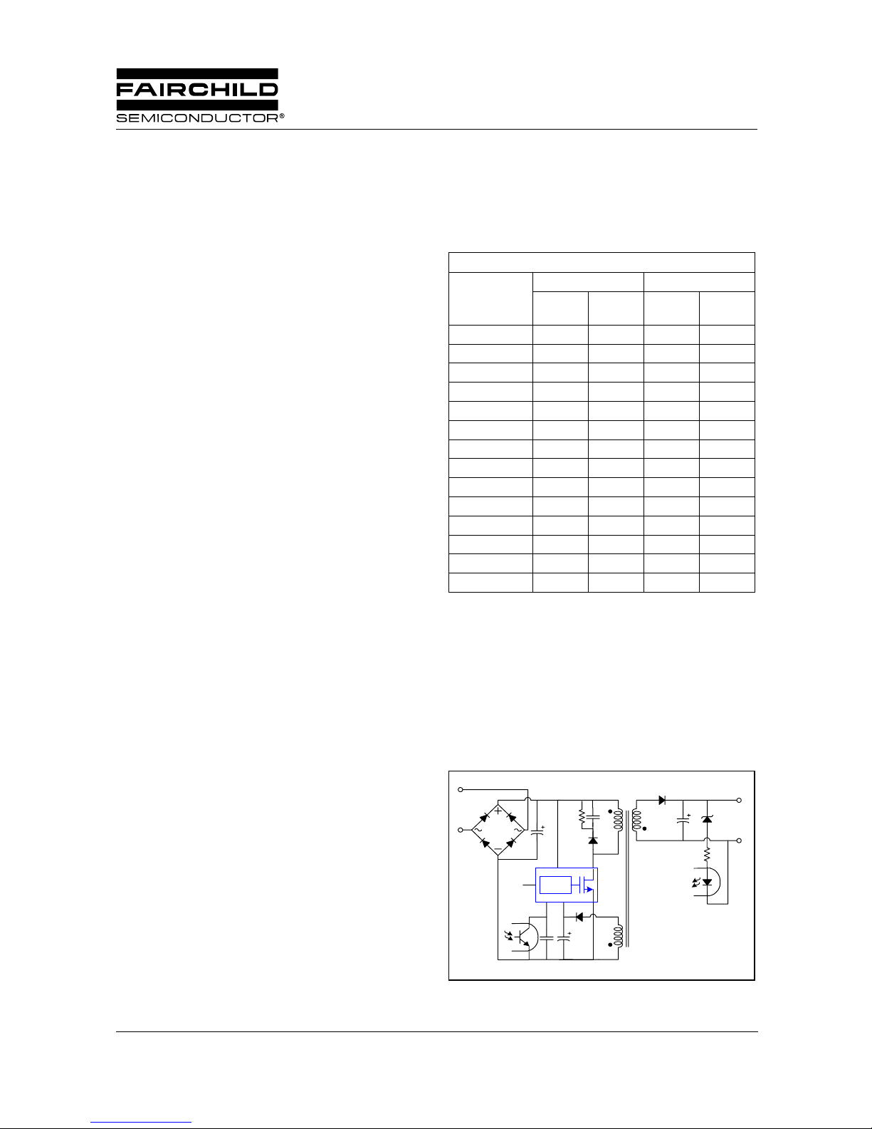
Typical Circuit
Figure 1. Typical Flyback Application
OUTPUT POWER TABLE
PRODUCT
230VAC ±15%
(3)
85-265VAC
Adapt-
er
(1)
Open
Frame
(2)
Adapt-
er
(1)
Open
Frame
(2)
FSDL321 11W 17W 8W 12W
FSDH321 11W 17W 8W 12W
FSDL0165RN 13W 23W 11W 17W
FSDM0265RN 16W 27W 13W 20W
FSDH0265RN 16W 27W 13W 20W
FSDL0365RN 19W 30W 16W 24W
FSDM0365RN 19W 30W 16W 24W
FSDL321L 11W 17W 8W 12W
FSDH321L 11W 17W 8W 12W
FSDL0165RL 13W 23W 11W 17W
FSDM0265RL 16W 27W 13W 20W
FSDH0265RL 16W 27W 13W 20W
FSDL0365RL 19W 30W 16W 24W
FSDM0365RL 19W 30W 16W 24W
Drain
Source
Vstr
Vfb Vcc
PWM
AC
IN
DC
OUT
Ipk
FSDH321, FSDL321
Green Mode Fairchild Power Switch (FPS
TM
)
Page 2
FSDH321, FSDL321
2
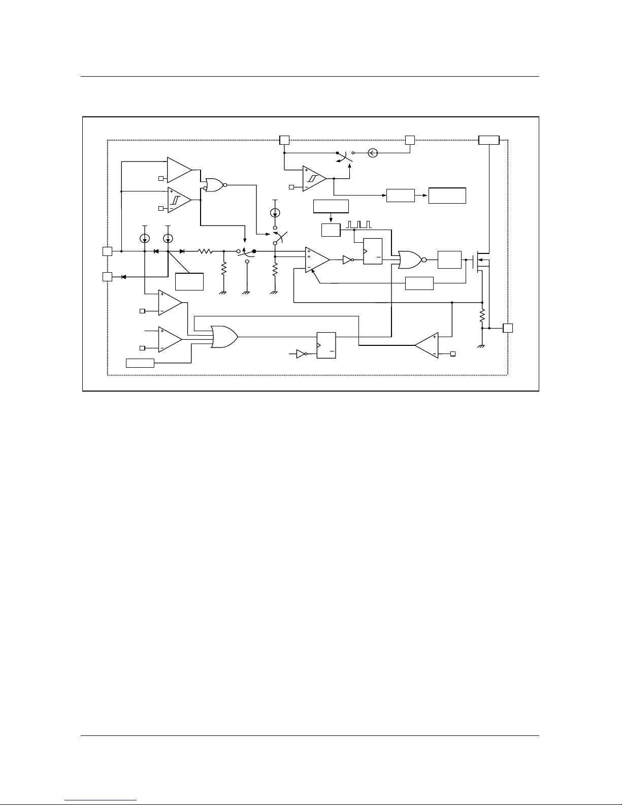
Internal Block Diagram
Figure 2. Functional Block Diagram of FSDx321
8V/12V
2 6,7,8
1
3
Vref
Internal
Bias
SQQ
R
OSC
Vcc Vcc
I
DELAY
I
FB
V
SD
TSD
Vovp
Vcc
Vocp
SQQ
R
R
2.5R
Vcc good
Vcc
Drain
Vfb
GND
AOCP
Gate
driver
5
Vstr
I
CH
Vcc good
VBURL/VBURH
LEB
PWM
+
-
4
Ipk
Freq.
Modulation
VBURH
Vcc
I
BUR(pk)
Burst
Normal
Soft
Start
Page 3
FSDH321, FSDL321
3
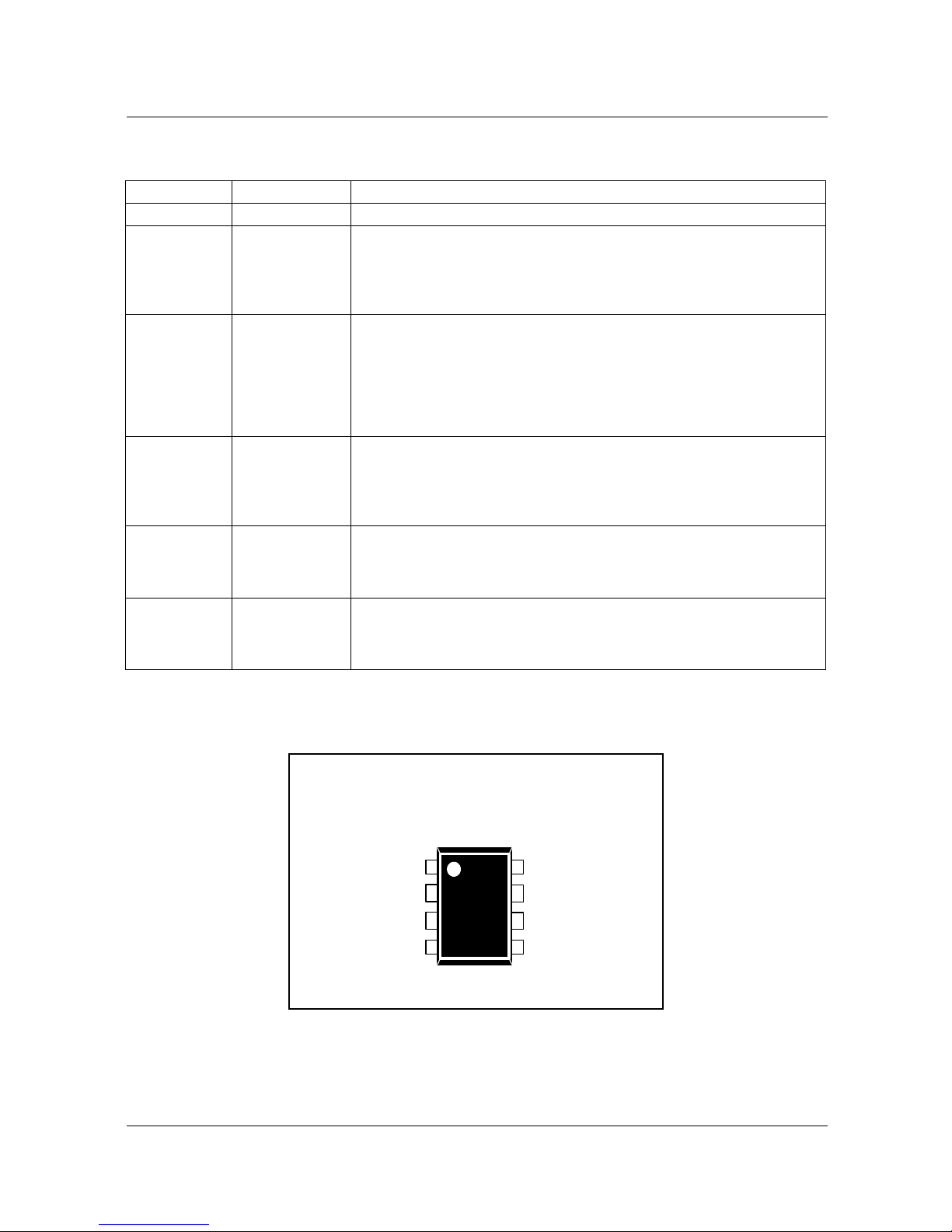
Pin Definitions
Pin Configuration
Figure 3. Pin Configuration (Top View)
Pin Number Pin Name Pin Function Description
1 GND Sense FET source terminal on primary side and internal control ground.
2Vcc
Positive supply voltage input. Although connected to an auxiliary transformer winding, current is supplied from pin 5 (Vstr) via an internal switch during
startup (see Internal Block Diagram section). It is not until Vcc reaches the
UVLO upper threshold (12V) that the internal start-up switch opens and device power is supplied via the auxiliary transformer winding.
3Vfb
The feedback voltage pin is the non-inverting input to the PWM comparator.
It has a 0.9mA current source connected internally while a capacitor and optocoupler are typically connected externally. A feedback voltage of 6V triggers over load protection (OLP). There is a time delay while charging
external capacitor Cfb from 3V to 6V using an internal 5uA current source.
This time delay prevents false triggering under transient conditions, but still
allows the protection mechanism to operate under true overload conditions.
4Ipk
This pin adjusts the peak current limit of the Sense FET. The feedback
0.9mA current source is diverted to the parallel combination of an internal
2.8kΩ resistor and any external resistor to GND on this pin to determine the
peak current limit. If this pin is tied to Vcc or left floating, the typical peak current limit will be 0.7A.
5Vstr
This pin connects directly to the rectified AC line voltage source. At start up
the internal switch supplies internal bias and charges an external storage
capacitor placed between the Vcc pin and ground. Once the Vcc reaches
12V, the internal switch is opened.
6, 7, 8 Drain
The drain pins are designed to connect directly to the primary lead of the
transformer and are capable of switching a maximum of 650V. Minimizing
the length of the trace connecting these pins to the transformer will decrease
leakage inductance.
1
2
3
45
6
7
8GND
Vcc
Vfb
Ipk
Vstr
Drain
Drain
Drain
8DIP
8LSOP
Page 4

FSDH321, FSDL321
4
Absolute Maximum Ratings
(Ta=25°C, unless otherwise specified)
Note:
1. Repetitive rating: Pulse width is limited by maximum junction temperature
2. L = 24mH, starting Tj = 25°C
Thermal Impedance
(Ta=25°C, unless otherwise specified)
Note:
1. Free standing with no heatsink; Without copper clad.
/ Measurement Condition : Just before junction temperature T
J
enters into OTP.
2. Measured on the DRAIN pin close to plastic interface.
- all items are tested with the standards JESD 51-2 and 51-10 (DIP).
Characteristic Symbol Value Unit
Drain Pin Voltage V
DRAIN
650 V
Vstr Pin Voltage V
STR
650 V
Drain-Gate Voltage V
DG
650 V
Gate-Source Voltage V
GS
±20
V
Drain Current Pulsed
(1)
I
DM
1.5 A
Continuous Drain Current (Tc=25℃) I
D
0.7 A
Continuous Drain Current (Tc=100℃) I
D
0.32 A
Single Pulsed Avalanche Energy
(2)
E
AS
10 mJ
Supply Voltage V
CC
20 V
Feedback Voltage Range V
FB
-0.3 to V
CC
V
Total Power Dissipation P
D
1.40 W
Operating Junction Temperature T
J
Internally limited °C
Operating Ambient Temperature T
A
-25 to +85 °C
Storage Temperature T
STG
-55 to +150 °C
Parameter Symbol Value Unit
8DIP
Junction-to-Ambient Thermal
(1)
θ
JA
88.84 °C/W
Junction-to-Case Thermal
(2)
θ
JC
13.94 °C/W
Page 5

FSDH321, FSDL321
5
Electrical Characteristics
(Ta = 25°C unless otherwise specified)
Note:
1. Pulse test: Pulse width ≤ 300us, duty ≤ 2%
2. These parameters, although guaranteed, are tested in EDS (wafer test) process
3. These parameters, although guaranteed, are not 100% tested in production
Parameter Symbol Condition Min. Typ. Max. Unit
SENSE FET SECTION
Zero-Gate-Voltage Drain Current I
DSS
VDS=650V, VGS=0V - - 25
µA
VDS=520V, VGS=0V, TC=125°C
- - 200
Drain-Source On-State Resistance
R
DS(ON) VGS
=10V, ID=0.5A - 14 19 Ω
Forward Trans-Conductance
(1)
g
fs
VDS=50V, ID=0.5A 1.0 1.3 - S
Input Capacitance C
ISS
VGS=0V, VDS=25V,
f=1MHz
- 162 pFOutput Capacitance C
OSS
-18-
Reverse Transfer Capacitance C
RSS
-3.8-
Turn-On Delay Time t
d(on)
V
DS
=325V, ID=1.0A
-9.5-
ns
Rise Time t
r
-19-
Turn-Off Delay Time t
d(off)
-33-
Fall Time t
f
- 42 -
Total Gate Charge Q
g
VGS=10V, ID=1.0A,
V
DS
=325V
-7.0nCGate-Source Charge Q
gs
-3.1-
Gate-Drain (Miller) Charge Q
gd
-0.4-
CONTROL SECTION
Switching Frequency f
OSC
FSDH321
90 100 110 KHz
Switching Frequency Modulation ∆f
MOD
±2.5 ±3.0 ±3.5 KHz
Switching Frequency f
OSC
FSDL321
45 50 55 KHz
Switching Frequency Modulation ∆f
MOD
±1.0 ±1.5 ±2.0 KHz
Switching Frequency Variation
(2)
∆f
OSC
-25°C ≤ Ta ≤ 85°C - ±5 ±10 %
Maximum Duty Cycle D
MAX
FSDH321 62 67 72 %
FSDL321 71 77 83 %
UVLO Threshold Voltage
V
START
VFB=GND 11 12 13 V
V
STOP
VFB=GND 7 8 9 V
Feedback Source Current I
FB
VFB=GND 0.7 0.9 1.1 mA
Internal Soft Start Time t
S/S
VFB=4V 10 15 20 ms
BURST MODE SECTION
Burst Mode Voltage
V
BURH
Tj=25°C
0.4 0.5 0.6 V
V
BURL
0.25 0.35 0.45 V
V
BUR(HYS)
Hysteresis - 150 - mV
PROTECTION SECTION
Peak Current Limit I
LIM
Tj=25°C, ∆i/∆t=250mA/us 0.60 0.70 0.80 A
Current Limit Delay Time
(3)
t
CLD
Tj=25°C - 600 - ns
Thermal Shutdown Temperature
(3)
TSD 125 145 -
°
C
Shutdown Feedback Voltage V
SD
5.5 6.0 6.5 V
Over Voltage Protection V
OVP
18 19 20 V
Shutdown Delay Current I
DELAY
VFB=4V 3.5 5.0 6.5 µA
Leading Edge Blanking Time t
LEB
200 - - ns
TOTAL DEVICE SECTION
Operating Supply Current
(control part only) I
OP
VCC=14V, VFB=0V 1 3 5 mA
Start-Up Charging Current I
CH
VCC=0V 0.7 0.85 1.0 mA
Vstr Supply Voltage V
STR
VCC=0V 35 - - V
Page 6

FSDH321, FSDL321
6
Comparison Between FSDM311 and FSDx321
Function FSDM311 FSDx321 FSDx321 Advantages
Soft-Start 15ms 15ms
(same for both devices)
• Gradually increasing current limit
during soft-start further reduces peak
current and voltage stresses
• Eliminates external components used
for soft-start in most applications
• Reduces or eliminates output
overshoot
External Current Limit not applicable Programmable of
default current limit
• Smaller transformer
• Allows power limiting (constant overload power)
• Allows use of larger device for lower
losses and higher efficiency.
Frequency Modulation not applicable ±3.0KHz @100KHz
±1.5KHz @50KHz
• Reduces conducted EMI
Burst Mode Operation Built into controller Built into controller
(same for both devices)
• Improves light load efficiency
• Reduces power consumption at noload
• Transformer audible noise reduction
Drain Creepage at
Package
7.62mm 7.62mm
(same for both devices)
• Greater immunity to arcing provoked
by dust, debris and other contaminants
Page 7

FSDH321, FSDL321
7
Typical Performance Characteristics (Control Part)
(These characteristic graphs are normalized at Ta = 25°C)
0.00
0.20
0.40
0.60
0.80
1.00
1.20
-50 0 50 100 150
Temp[℃]
Normalized
Operating Frequency (Fosc) vs. Ta
0.00
0.20
0.40
0.60
0.80
1.00
1.20
-50 0 50 100 150
Temp[℃]
Normalized
Frequency Modulation (∆FMOD) vs. Ta
0.00
0.20
0.40
0.60
0.80
1.00
1.20
-50 0 50 100 150
Temp[℃]
Normalized
Maximum Duty Cycle (D
MAX
) vs. Ta
0.00
0.20
0.40
0.60
0.80
1.00
1.20
-50 0 50 100 150
Temp[℃]
Normalized
Operating Supply Current (I
OP
) vs. Ta
0.00
0.20
0.40
0.60
0.80
1.00
1.20
-50 0 50 100 150
Temp[℃]
Normalized
Start Threshold Voltage (V
START
) vs. Ta
0.00
0.20
0.40
0.60
0.80
1.00
1.20
-50 0 50 100 150
Temp[℃]
Normalized
Stop Threshold Voltage (V
STOP
) vs. Ta
Page 8

FSDH321, FSDL321
8
Typical Performance Characteristics (Continued)
0.00
0.20
0.40
0.60
0.80
1.00
1.20
-50 0 50 100 150
Temp[℃]
Normalized
Feedback Source Current (IFB) vs. Ta
0.00
0.20
0.40
0.60
0.80
1.00
1.20
-50 0 50 100 150
Temp[℃]
Normalized
Peak Current Limit (I
LIM
) vs. Ta
0.00
0.20
0.40
0.60
0.80
1.00
1.20
-50 0 50 100 150
Temp[℃]
Normalized
Start Up Charging Current (ICH)
vs. Ta
0.00
0.20
0.40
0.60
0.80
1.00
1.20
-50 0 50 100 150
Temp[℃]
Normalized
Burst Peak Current (I
BUR(pk)
) vs. Ta
0.00
0.20
0.40
0.60
0.80
1.00
1.20
-50 0 50 100 150
Temp[℃]
Normalized
Over Voltage Protection (V
OVP
) vs. Ta
Page 9
FSDH321, FSDL321
9
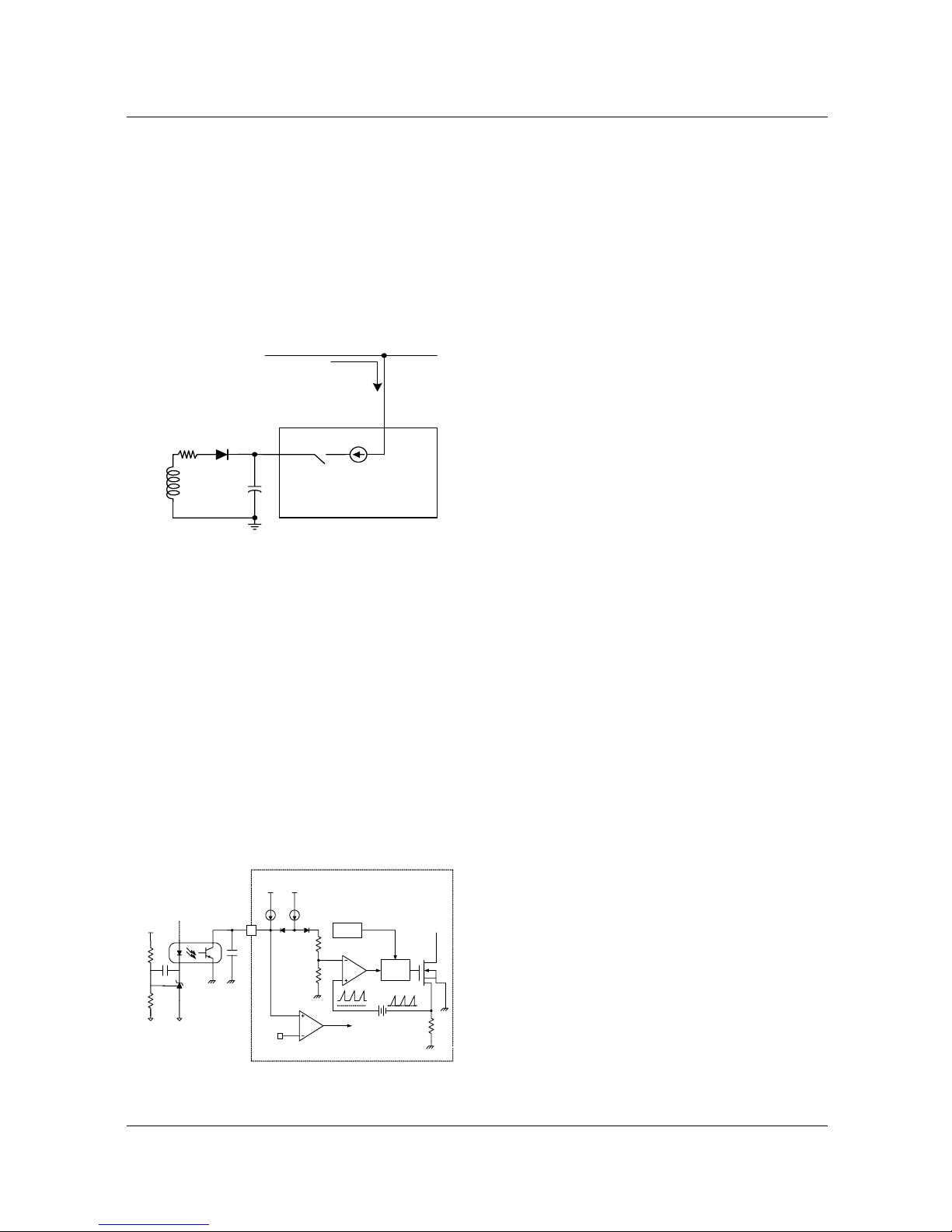
Functional Description
1. Startup : In previous generations of Fairchild Power
Switches (FPS
TM
) the Vstr pin had an external resistor to the
DC input voltage line. In this generation the startup resistor
is replaced by an internal high voltage current source and a
switch that shuts off when 15ms goes by after the supply
voltage, Vcc, gets above 12V. The source turns back on if
Vcc drops below 8V.
Figure 4. High Voltage Current Source
2. Feedback Control : The FSDx321 employs current mode
control, as shown in Figure 5. An opto-coupler (such as the
H11A817A) and shunt regulator (such as the KA431) are
typically used to implement the feedback network. Comparing the feedback voltage with the voltage across the Rsense
resistor plus an offset voltage makes it possible to control the
switching duty cycle. When the KA431 reference pin voltage exceeds the internal reference voltage of 2.5V, the optocoupler LED current increases, the feedback voltage Vfb is
pulled down and it reduces the duty cycle. This event typically happens when the input voltage is increased or the output load is decreased.
Figure 5. Pulse Width Modulation (PWM) Circuit
3. Leading Edge Blanking (LEB) : At the instant the internal Sense FET is turned on, the primary side capacitance and
secondary side rectifier diode reverse recovery typically
cause a high current spike through the Sense FET. Excessive
voltage across the Rsense resistor leads to incorrect feedback
operation in the current mode PWM control. To counter this
effect, the FPS employs a leading edge blanking (LEB) circuit. This circuit inhibits the PWM comparator for a short
time (t
LEB
) after the Sense FET is turned on.
4. Protection Circuits : The FPS has several protective
functions such as over load protection (OLP), over voltage
protection (OVP), abnormal over current protection
(AOCP), under voltage lock out (UVLO) and thermal shutdown (TSD). Because these protection circuits are fully integrated inside the IC without external components, the
reliability is improved without increasing cost. Once a fault
condition occurs, switching is terminated and the Sense FET
remains off. This causes Vcc to fall. When Vcc reaches the
UVLO stop voltage V
STOP
(8V), the protection is reset and
the internal high voltage current source charges the Vcc
capacitor via the Vstr pin. When Vcc reaches the UVLO
start voltage V
START
(12V), the FPS resumes its normal
operation. In this manner, the auto-restart can alternately
enable and disable the switching of the power Sense FET
until the fault condition is eliminated.
4.1 Over Load Protection (OLP) : Overload is defined as
the load current exceeding a pre-set level due to an unexpected event. In this situation, the protection circuit should
be activated in order to protect the SMPS. However, even
when the SMPS is operating normally, the over load protection (OLP) circuit can be activated during the load transition.
In order to avoid this undesired operation, the OLP circuit is
designed to be activated after a specified time to determine
whether it is a transient situation or an overload situation. In
conjunction with the Ipk current limit pin (if used) the current mode feedback path would limit the current in the Sense
FET when the maximum PWM duty cycle is attained. If the
output consumes more than this maximum power, the output
voltage (Vo) decreases below its rating voltage. This reduces
the current through the opto-coupler LED, which also
reduces the opto-coupler transistor current, thus increasing
the feedback voltage (V
FB
). If VFB exceeds 3V, the feed-
back input diode is blocked and the 5uA current source (I
DE-
LAY
) starts to charge Cfb slowly up to Vcc. In this condition,
V
FB
increases until it reaches 6V, when the switching operation is terminated as shown in Figure 6. The shutdown delay
time is the time required to charge Cfb from 3V to 6V with
5uA current source.
Vin,dc
Vstr
Vcc
15ms a fter
Vcc≥12V
UVLO off
Vcc<8V
UVLO on
I
STR
J-FET
I
CH
3
OSC
Vcc Vcc
5uA 0.9mA
V
SD
R
2.5R
Gate
driver
OLP
D1 D2
V
FB
Vfb
431
C
FB
Vo
+
-
V
FB,in
Page 10

FSDH321, FSDL321
10
Figure 6. Over Load Protection (OLP)
4.2 Thermal Shutdown (TSD) : The Sense FET and the
control IC are integrated, making it easier for the control IC
to detect the temperature of the Sense FET. When the temperature exceeds approximately 145°C, thermal shutdown is
activated.
4.3 Abnormal Over Current Protection (AOCP) : Even
though the FPS has OLP (Over Load Protection) and current
mode PWM feedback, these are not enough to protect the
FPS when a secondary side diode short or a transformer pin
short occurs. In addition to start-up, soft-start is also
activated at each restart attempt during auto-restart and when
restarting after latch mode is activated. The FPS has an
internal AOCP (Abnormal Over Current Protection) circuit,
as shown in Figure 7. When the gate turn-on signal is applied
to the power Sense FET, the AOCP block is enabled and
monitors the current through the sensing resistor. The
voltage across the resistor is then compared with a preset
AOCP level. If the sensing resistor voltage is greater than the
AOCP level, pulse-by-pulse AOCP is triggered regardless of
uncontrollable LEB time. Here, pulse-by-pulse AOCP stops
the Sense FET within 350ns after it is activated.
Figure 7. Abnormal Over Current Protection (AOCP)
4.4 Over Voltage Protection (OVP) : In the event of a malfunction in the secondary side feedback circuit, or an open
feedback loop caused by a soldering defect, the current
through the opto-coupler transistor becomes almost zero
(refer to Figure 5). Then, V
FB
climbs up in a similar manner
to the over load situation, forcing the preset maximum current to be supplied to the SMPS until the over load protection
is activated. Because excess energy is provided to the output,
the output voltage may exceed the rated voltage before the
over load protection is activated, resulting in the breakdown
of the devices in the secondary side. In order to prevent this
situation, an over voltage protection (OVP) circuit is
employed. In general, Vcc is proportional to the output voltage and the FPS uses Vcc instead of directly monitoring the
output voltage. If V
CC
exceeds 19V, OVP circuit is activated
resulting in termination of the switching operation. In order
to avoid undesired activation of OVP during normal operation, Vcc should be properly designed to be below 19V.
V
FB
t
3V
6V
Over Load Protection
t12= C
FB
×
(V(t2)-V(t1)) / I
DELAY
t
1
t
2
VtVVtVAI
I
tVtV
Ct
DELAY
DELAY
FB
6)(,3)(,5;
)()(
21
12
12
===
−
=
µ
Vsense
V
FB,in
Gate Driver
Rsense
CLK
Drain
V
AOCP
PWM
COMPARATOR
AOCP
COMPARATOR
LEB
R
SQ
Page 11

FSDH321, FSDL321
11
5. Soft Start : The FPS has an internal soft start circuit that
slowly increases the feedback voltage together with the
Sense FET current after it starts up. The typical soft start
time is 15msec, as shown in Figure 8, where progressive
increments of the Sense FET current are allowed during the
start-up phase. The pulse width to the power switching
device is progressively increased to establish the correct
working conditions for transformers, inductors, and capacitors. The voltage on the output capacitors is progressively
increased with the intention of smoothly establishing the
required output voltage. It also helps to prevent transformer
saturation and reduce the stress on the secondary diode.
Figure 8. Soft Start Function
6. Burst Operation : In order to minimize power dissipation
in standby mode, the FPS enters burst mode operation. As
the load decreases, the feedback voltage decreases. As
shown in Figure 9, the device automatically enters burst
mode when the feedback voltage drops below
V
BURH
(500mV). Switching still continues but the current
limit is set to a fixed limit internally to minimize flux density
in the transformer. The fixed current limit is larger than that
defined by V
FB
= V
BURH
and therefore, VFB is driven
down further. Switching continues until the feedback voltage
drops below V
BURL
(350mV). At this point switching stops
and the output voltages start to drop at a rate dependent on
the standby current load. This causes the feedback voltage to
rise. Once it passes V
BURH
(500mV), switching resumes.
The feedback voltage then falls and the process repeats.
Burst mode operation alternately enables and disables
switching of the power Sense FET thereby reducing switching loss in Standby mode.
Figure 9. Burst Operation Function
7. Frequency Modulation : Modulating the switching frequency of a switched power supply can reduce EMI. Frequency modulation can reduce EMI by spreading the energy
over a wider frequency range than the bandwidth measured
by the EMI test equipment. The amount of EMI reduction is
directly related to the depth of the reference frequency. As
can be seen in Figure 10, the frequency changes from 97KHz
to 103KHz in 4ms for the FSDH321 (48.5KHz to 51.5KHz
for FSDL321). Frequency modulation allows the use of a
cost effective inductor instead of an AC input mode choke to
satisfy the requirements of world wide EMI limits.
Figure 10. Frequency Modulation Waveform
1ms
15steps
Current limit
0.4A
0.7A
t
Drain current
V
BURH
Switching
OFF
Current
Waveform
Burst
Operation
Normal
Operation
V
FB
V
BURL
Switching
OFF
Burst
Operation
3
Vcc Vcc
I
DELAY
I
FB
R
2.5R
Vfb
VBURL/VBURH
PWM
+
-VBURH
Vcc
I
BUR(pk)
Burst
Normal
MOSFET
Current
t
s
fs=1/t
s
100kHz
103kHz
97kHz
4ms
t
Drain
Current
Page 12

FSDH321, FSDL321
12
Figure 11. KA5-series FPS Full Range EMI scan(67KHz,
no Frequency Modulation) with DVD Player SET
Figure 12. FSDX-series FPS Full Range EMI Scan (67KHz,
with Frequency Modulation) with DVD Player SET
8. Adjusting Peak Current Limit : As shown in Figure 13,
a combined 2.8kΩ internal resistance is connected to the
non-inverting lead on the PWM comparator. A external
resistance of Rx on the current limit pin forms a parallel
resistance with the 2.8kΩ when the internal diodes are
biased by the main current source of 900uA.
Figure 13. Peak Current Limit Adjustment
For example, FSDx321 has a typical Sense FET peak current
limit (I
LIM
) of 0.7A. I
LIM
can be adjusted to 0.5A by inserting Rx between the Ipk pin and the ground. The value of the
Rx can be estimated by the following equations:
0.7A : 0.5A = 2.8kΩ : XkΩ ,
X = Rx || 2.8kΩ .
(X represents the resistance of the parallel network)
Frequency (MHz)
Amplitude (dBµV)
Frequency (MHz)
Amplitude (dBµV)
3
Vcc V cc
I
DELAY
I
FB
2k
Ω
Vfb
PWM
Comparator
4
Ipk
0.8k
Ω
Rx
SenseFET
Current
Sense
900uA5uA
Page 13

FSDH321, FSDL321
13
Application Tips
1. Methods of Reducing Audible Noise
Switching mode power converters have electronic and
magnetic components, which generate audible noises when
the operating frequency is in the range of 20~20,000 Hz.
Even though they operate above 20 kHz, they can make
noise depending on the load condition. Designers can
employ several methods to reduce these noises. Here are
three of these methods:
Glue or Varnish
The most common method involves using glue or varnish
to tighten magnetic components. The motion of core, bobbin
and coil and the chattering or magnetostriction of core can
cause the transformer to produce audible noise. The use of
rigid glue and varnish helps reduce the transformer noise.
But, it also can crack the core. This is because sudden
changes in the ambient temperature cause the core and the
glue to expand or shrink in a different ratio according to the
temperature.
Ceramic Capacitor
Using a film capacitor instead of a ceramic capacitor as a
snubber capacitor is another noise reduction solution. Some
dielectric materials show a piezoelectric effect depending on
the electric field intensity. Hence, a snubber capacitor
becomes one of the most significant sources of audible
noise. It is considerable to use a zener clamp circuit instead
of an RCD snubber for higher efficiency as well as lower
audible noise.
Adjusting Sound Frequency
Moving the fundamental frequency of noise out of 2~4 kHz
range is the third method. Generally, humans are more sensitive to noise in the range of 2~4 kHz. When the fundamental
frequency of noise is located in this range, one perceives the
noise as louder although the noise intensity level is identical.
Refer to Figure 14. Equal Loudness Curves.
When FPS acts in Burst mode and the Burst operation is
suspected to be a source of noise, this method may be helpful. If the frequency of Burst mode operation lies in the
range of 2~4 kHz, adjusting feedback loop can shift the
Burst operation frequency. In order to reduce the Burst operation frequency, increase a feedback gain capacitor (C
F
),
opto-coupler supply resistor (R
D
) and feedback capacitor
(C
B
) and decrease a feedback gain resistor (RF) as shown in
Figure 15. Typical Feedback Network of FPS.
Figure 14. Equal Loudness Curves
Figure 15. Typical Feedback Network of FPS
2. Other Reference Materials
AN-4134: Design Guidelines for Off-line Forward Convert-
ers Using Fairchild Power Switch (FPS
TM
)
AN-4137: Design Guidelines for Off-line Flyback Convert-
ers Using Fairchild Power Switch (FPS)
AN-4140: Transformer Design Consideration for Off-line
Flyback Converters using Fairchild Power Switch
(FPS
TM
)
AN-4141: Troubleshooting and Design Tips for Fairchild
Power Switch (FPS
TM
) Flyback Applications
AN-4147: Design Guidelines for RCD Snubber of Flyback
AN-4148: Audible Noise Reduction Techniques for FPS
Applications
Page 14

FSDH321, FSDL321
14
Typical Application Circuit
Features
• High efficiency (>70% at full load, full input range)
• Low standby mode power consumption (<1W at DC 375V input and 0.5W load)
• Low component count
• Enhanced system reliability through various protection functions
• Low EMI through frequency modulation
• Internal soft-start (15ms)
Key Design Notes
• The delay time for over load protection is designed to be about 13ms with C104 of 22nF. If faster/slower triggering of OLP
is required, C104 can be changed to a smaller/larger value(eg. 47nF for about 30ms).
• The pule-by-pulse peak current limit level(I
LIM
) is set to default value 0.7A by floating the Ipk pin (#4).
• R102 and C101 clamp the DRAIN voltage of MOSFET below 650V under all conditions.
1. Schematic
Application Output power Input voltage Output voltage (Max current)
PC Auxiliary
Power Supply
10W DC 140~375V 5.0V (2.0A)
10W PC Auxiliary Power Circuit
T1
EE1625
7
10
D201
SB360
C201
1000uF
16V
C203
470uF
16V
L201
10uH
5V
(+/-5%)
2A
C101
10nF
630V
1
2
4
5
R102
100kΩ
1W
D101
UF 4007
C104
22nF
C103
10uF
50V
D103
1N 4937
R104
10Ω
R202
330Ω
R201
1kΩ
R203
2kΩ
C202
100nF
R204
2kΩ
IC 301
H11A817A
IC201
KA431
3
Vfb
Vcc
Drain
GND
6
140~375
VDC
INPUT
IC101
FSDx321
6,7,8
1
2
3
R103
10Ω
D102
1N4937
C102
47uF
50V
M Vcc
C301
2.2n F
Vstr
5
R101
680kΩ
1W
ZD1
18V
ZD2
18V
Page 15

FSDH321, FSDL321
15
2. Transformer Schematic Diagram
3. Winding Specification
4. Electrical Characteristics
5. Core & Bobbin
Core : EER1625
Bobbin : EER1625
EE1625
N
p
/2
N
a
1
2
3
4
5
6
7
8
N
5V
N
M Vcc
9
10
N
p
/2
N
a
N
M Vcc
N
5V
Np/2
Np/2
Pin(S → F) Wire Turns Winding Method
Np/2 3 → 2 0.15φ × 1 80 So leno id w ind ing
Ins ulation : P o lye ster T a pe t = 0 .05 0 m m , 3L aye rs
N5V 10 → 7 0.55φ ×1 12 Solenoid winding
Ins ulation : P o lye ster T a pe t = 0 .05 0 m m , 3L aye rs
N
MVcc
4 → 6 0.20φ ×1 40 So leno id w inding
Ins ulation : P o lye ster T a pe t = 0 .05 0 m m , 3L aye rs
N
P/2
2 → 1 0.15 φ ×1 8 0 So len oid w in ding
Ins ulation : P o lye ster T a pe t = 0 .05 0 m m , 3L aye rs
Na 5 → 6 0 .20φ ×1 34 So len o id w inding
Oute r In sula tion : P olye ste r T a pe t = 0.05 0m m , 3 Lay ers
Pin Spec. Remark
Indu cta n c e 1- 3 1 .8 m H 1k H z , 1 V
Leakage 1- 3 100 uH 2nd side all short
Page 16

FSDH321, FSDL321
16
6. Demo Circuit Part List
Part Value Note Part Value Note
Resistor Inductor
R101 680K 1W L201 10uH -
R102 100K 1W -
R103 10 1/4W Diode
R104 10 1/4W D101 UF4007 PN Ultra Fast
R201 1K 1/4W D102 1N4937 PN Ultra Fast
R202 330 1/4W D103 1N4937 PN Ultra Fast
R203 2K 1/4W D201 SB360 Schottky
R204 2K 1/4W ZD1 1N4746A 18V Zener
ZD2 1N4746A 18V Zener
Capacitor
C101 10nF/630V Film
IC
C102 47uF/50V Electrolytic IC101 FSDH321 FPS™
C103 10uF/50V Electrolytic IC201 KA431(TL431)
Voltage
reference
C104 22nF/50V Film IC301 H11A817A
Opto-Coupler
C201 1000uF/16V Electrolytic
C202 100nF/50V Ceramic
C203 1uF/100V Electrolytic
C204 470uF/16V Electrolytic
C301 2.2nF/35V Ceramic
Page 17

FSDH321, FSDL321
17
Package Dimensions
8DIP
Page 18
FSDH321, FSDL321
18
Package Dimensions (Continued)
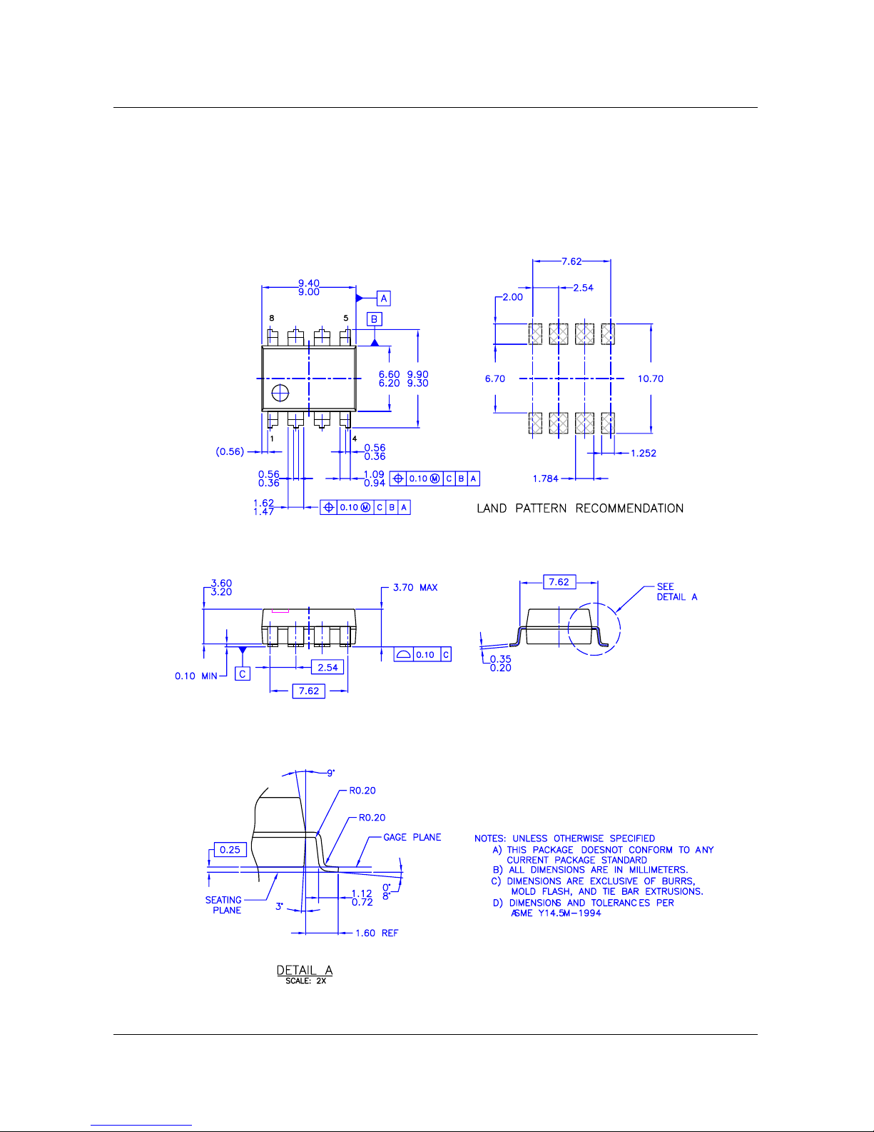
8LSOP
Page 19

FSDH321, FSDL321
19
Ordering Information
Product Number Package Marking Code BV
DSS
f
OSC
R
DS(ON)
FSDH321 8DIP DH321 650V 100KHz 14Ω
FSDL321 8DIP DL321 650V 50KHz 14Ω
FSDH321L 8LSOP DH321 650V 100KHz 14Ω
FSDL321L 8LSOP DL321 650V 50KHz 14Ω
Page 20

FSDH321, FSDL321
9/29/05 0.0m 001
© 2005 Fairchild Semiconductor Corporation
LIFE SUPPORT POLICY
FAIRCHILD’S PRODUCTS ARE NOT AUTHORIZED FOR USE AS CRITICAL COMPONENTS IN LIFE SUPPORT DEVICES
OR SYSTEMS WITHOUT THE EXPRESS WRITTEN APPROVAL OF THE PRESIDENT OF FAIRCHILD SEMICONDUCTOR
CORPORATION. As used herein:
1. Life support devices or systems are devices or systems
which, (a) are intended for surgical implant into the body,
or (b) support or sustain life, and (c) whose failure to
perform when properly used in accordance with
instructions for use provided in the labeling, can be
reasonably expected to result in a significant injury of the
user.
2. A critical component in any component of a life support
device or system whose failure to perform can be
reasonably expected to cause the failure of the life support
device or system, or to affect its safety or effectiveness.
www.fairchildsemi.com
DISCLAIMER
FAIRCHILD SEMICONDUCTOR RESERVES THE RIGHT TO MAKE CHANGES WITHOUT FURTHER NOTICE TO ANY
PRODUCTS HEREIN TO IMPROVE RELIABILITY, FUNCTION OR DESIGN. FAIRCHILD DOES NOT ASSUME ANY
LIABILITY ARISING OUT OF THE APPLICATION OR USE OF ANY PRODUCT OR CIRCUIT DESCRIBED HEREIN; NEITHER
DOES IT CONVEY ANY LICENSE UNDER ITS PATENT RIGHTS, NOR THE RIGHTS OF OTHERS.
 Loading...