


www.fairchildsemi.com
FPS™Fairchild’s Power Switch for
Switch Mode Power Supply
Design Guide
FPS
Fairchild Semiconductor
™
Design Guide
Building Block
Solutions for
Multi-Market
Applications


FPS™Design Guide
Table Of Contents
What is Fairchild Power Switch FPS™ .......................................................................................................5
FPS™ Integrated Solution .........................................................................................................................6
Green FPS™ – New FPS™ Family.............................................................................................................7
Green FPS™ Features and Advantages......................................................................................................8
Burst Mode Operation .......................................................................................................................9
Frequency Modulation for EMI..........................................................................................................10
Over Load Protection .......................................................................................................................11
FPS™ Core Products..............................................................................................................................12
Complete FPS™ Product Offering Sorted by Output Power.........................................................................13
Typical Applications ..............................................................................................................................14
Examples of Typical Application Circuits .............................................................................................15-26
1W Power Supply with Less Than 100mW Standby Power..................................................................15
Dual Negative Output Non-Isolated Flyback .......................................................................................16
2.5W Single Output Isolated Flyback Using FSD200 with KA431 Reference .........................................17
10W Single Output Isolated Flyback Using FSDM0265R and Zener Diode ...........................................18
10W Multiple Output Isolated Flyback Using FSD210 with Primary Side Regulation ...............................19
5W Buck Converter Using FSDL0165RN ...........................................................................................20
16W Multiple Output Isolated Flyback Converter Using FSDM0265RN.................................................21
180W–200W KA5Q1265RF Quasi-resonant Flyback with Input Power
Factor Correction Using FAN7527B/FQP13N50C.........................................................................22-23
40W Isolated Flyback Power Supply
.................................................................................................24
24W Single Output 48V DC/DC Flyback Converter ...........................................................................25
Secondar
y Side Synchr
onous Rectification in a Power Over Ethernet Application ...................................26
Design Tools .........................................................................................................................................27
Ordering Guide ....................................................................................................................................28
www
.fair
childsemi.com/fps
3


FPS™Design Guide
What is Fairchild Power Switch (FPS™)
When you plug into a power receptacle anywhere in the world, more than likely the plug you are holding links
you to an off-line AC to DC power converter. The heart of today’s off-line converter is an integrated circuit (IC)
that not only contains the Pulse Width Modulation (PWM) circuitry and a power MOSFET converter that is
required for efficient conversion from AC to DC but also integrates a myriad of control and protection circuitry
that makes yesterday’s off-line converters bulky by comparison. Fairchild Power Switch (FPS™) is a family of
products that combines the avalanche rugged power SenseFET with state-of-the-art PWM circuitry to address a
variety of Switch Mode Power Supplies (SMPS).
An FPS™ IC contains protection against excessive heating within the converter, overloading of any DC output,
excessive currents that could damage the power MOSFET and excessive voltage of controlled DC output. These
necessary protection features are combined with advanced control features such as burst mode operation for
low standby power, a precision oscillator with frequency modulation to minimize EMI, and soft start.
Fairchild offers two design approaches:
1) Parallel dice, with SenseFET and PWM die side-by-side in one package,
2) Single die, monolithic design
The choice of these approaches allow cost-effective designs for a broad range of applications that include
chargers, adapters, set top boxes, VCR, DVD players, LCD and CRT TVs, LCD and CRT monitors, white goods,
PCs, notebooks and assorted household appliances.
The integration level is optimal and minimizes component count and saves board space. The FPS™ concept
provides cost-effective solutions for Flyback and Forward Converter topologies with outstanding reliability.
Combined with years of manufacturing expertise, these state-of-the-art off-line power switching solutions provide
the designers with the ability to do rapid production ramp-ups of their advanced SMPS design.
www
.fair
childsemi.com/fps
5
FPS™Design Guide
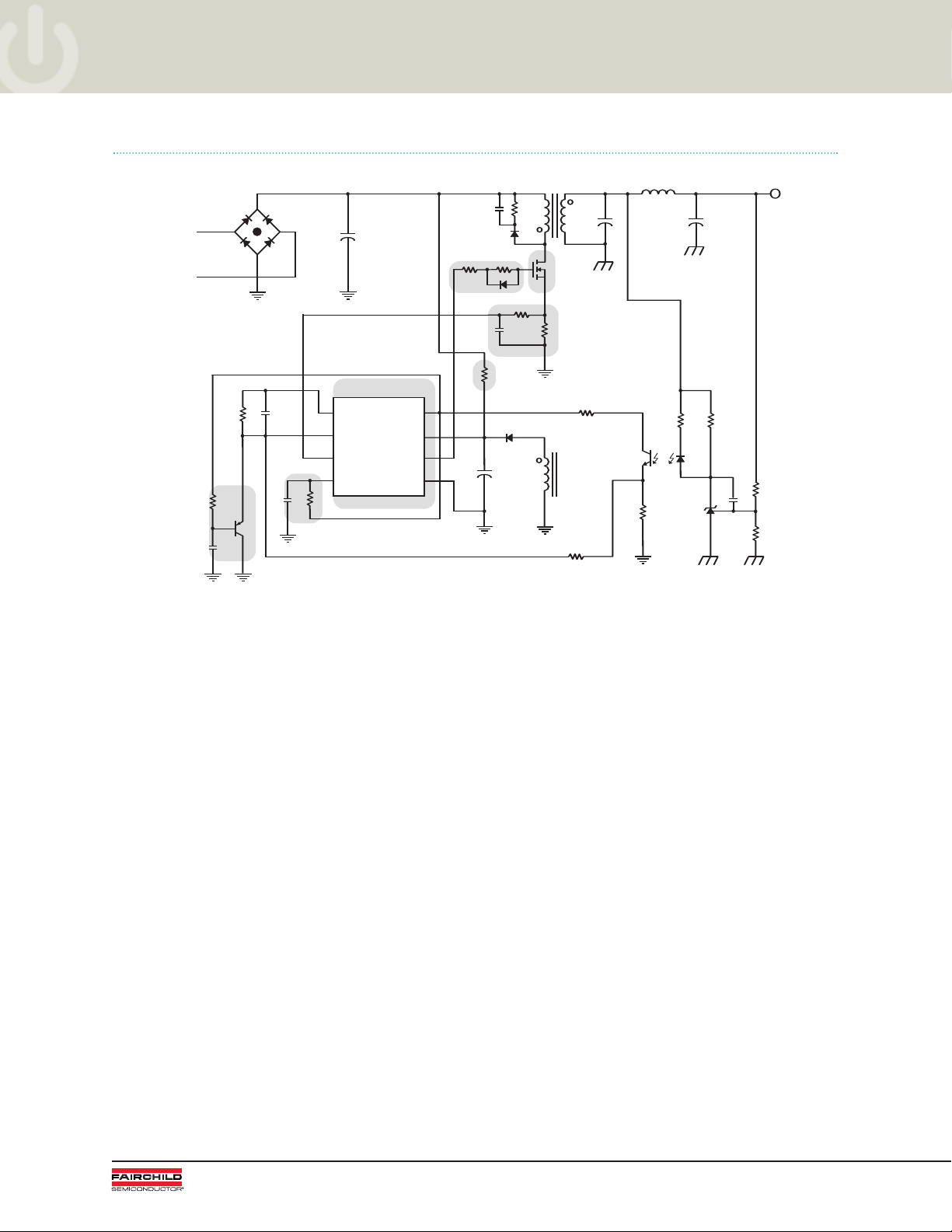
+
–
~~
AC
Input
Vo
Softstart
Frequency
Setting
Current
Sensing
MOSFET
Drive
PWM
Controller
Startup
Resistor
MOSFET
UC3842
Comp
Vref
RtCt
Isense
Vfb
Vcc
Out
GND
FPS™ Integrated Solution
Optimally Integrated Solution for Off-Line Switch Mode Power Supplies
• Integrated features in a single package
– SenseFET
– PWM controller
– Gate drive circuit
equency oscillator
ecise fr
– Pr
• Additional functions
– Startup circuit with soft start
– Frequency modulation
– Burst operation
• Protection function
– Over load protection
– Over voltage protection
– Over current protection
ent limit
– Pulse by pulse cur
– Over temperature protection
r
6
www
.fair
childsemi.com/fps

Green FPS™ – New FPS™ Family
Output Power GreenFPS™
Additional Features Application Example
Level Part Number
Low Power FSD200 Self biasing (FSD200) Charger
FSD210 Frequency modulation Auxiliary supply (for small display or controller
FS
DM311 Burst mode
boards in white goods for example)
FS
DL312 Built-in startup
Soft start
Medium Power
FSD1000 Auxiliary supplies PC main supply and PC auxiliary supply
(FPS with main power PWM integrated)
Burst mode
Programmable soft start
Internal startup
FS
DL0165RN Frequency modulation DVD player and auxiliary supply
FS
DH0265RN Built-in startup DVD player
FS
DM0265RN Soft start Digital Still Camera (DSC)
FSDL0365RN Burst mode DVD R/W
FSDM0365RN Programmable current limit LCD monitor
Digital Still Camera (DSC)
Set top box
FSDM0565R Bulit-in startup LCD monitor
FSDM07652R Soft start Notebook adapter
Burst mode Set top box
High Power FSCQ0765RT* Burst mode Color TV
FSCQ15658RT* Reducing IC current DVD receiver
Maximum frequency limit Plasma display panel
Soft start with fast settling
* Product in development
FPS™Design Guide
Green FPS™ is a New Family of FPS™ Products:
• Used in low standby power applications that meet the less than
att standar
1 W
• Suppor
• Integrated solution of multiple protection and control features built with the power
www
ts envir
switch MOSFET available in a very small package
.fair
childsemi.com/fps
ds (i.e. EnergyStar)
onmentally friendly systems
7

FPS™Design Guide
Snubber
Circuit
Load
+
+
++
Feedback
Circuit
Control
IC
FPS™
FPS™ Parallel Dice Solution
(Side-by- Side)
GNDVccIpk FB
Drain
Drain
Vstr Drain
SenseFET
PWM
IC
FPS™ Single Die Solution
(BCDMOS)
GND
GNDVFB GND
Vstr
Drain
Vcc
Green FPS™ Features and Advantages
Simplified Application Cir
cuit for FPS
™
Featur
es
• Optimal Solution for Off-Line SMPS
• Integrated Avalanche Rugged SenseFET
• Pulse-by-Pulse Current Limiting
• Various Protection Functions
(Over Voltage, Over Load, Over
Current, Thermal Shutdown)
• Burst Mode Operation for Low
Standby Power
• Frequency Modulation for Reduced EMI
• Soft Start Function
• Operation Fr
equency Options
(50/70/100/134kHz)
• External Frequency Synchronization
• Quasi Resonant
Advantages
• Low Standby Consumption with Burst Mode Operation
• Fully Avalanche Rugged, 650V and 800V SenseFETs Improves Reliability
Reduced EMI with Fully Integrated Frequency Modulation
•
• Reduces the Total Bill-of-Materials Cost with Integrated Protection and Control Functions
oad Application Coverage with Extensive Exper
• Br
tise and Easy-to-Use Design T
8
ools
www
.fair
childsemi.com/fps
FPS™Design Guide
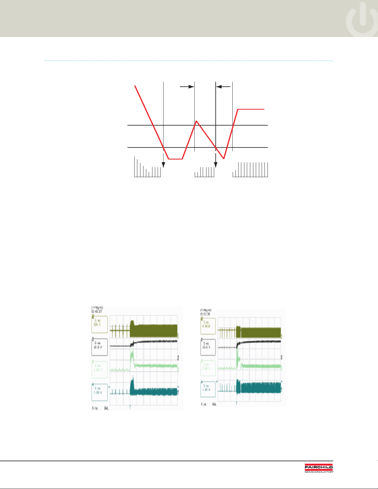
Current
Waveform
Feedback
Waveform
Burst
Operation
Normal Operation
Not
Switching
Not
Switching
V
BURSTH
V
BURSTL
standby normal
standby normal
Burst Operation @ 85VAC Burst Operation @ 265VAC
Green FPS™ Feature – Burst Mode Operation
(Refer to schematic in Typical Application Circuit 40W Isolated Flyback Power Supply on page 24)
• In standby mode, outputs draw very little to no load current
• Output voltages increase causing the feedback voltage to decrease
• When the feedback voltage goes below VBURSTL threshold, switching stops in the FPS device
saving considerable power
• Depending on load current, the output voltages will eventually fall causing the feedback voltage to increase
• Once the feedback voltage crosses VBURSTH threshold, switching starts again
• A 5V output FSD210 board at 265V in no load standby consumes a mere 92mW
Below shows the waveforms of both normal and standby modes at the voltage extremes for the universal
voltage range.
childsemi.com/fps
.fair
www
9

FPS™Design Guide
130kHz
131kHz
132kHz
133kHz
134kHz
135kHz
136kHz
137kHz
138kHz
2mS
A
B
C
130kHz134kHz
138kHz
Sawtooth
Waveform
Ton
Vfb
Vdrain
Idrain
A
B
C
100kHz Fixed Frequency
FSDH0165
134kHz with Frequency Modulation
FSD210
Peak Level Limit
Peak Level Limit
Peak Waveform
Quasi Peak Waveform
Green FPS™ Feature – Frequency Modulation for EMI
• Fixed frequency oscillators generate Electromagnetic
Interference (EMI) in a narrow band of the frequency spectrum
• Fairchild’s latest FPS devices modulate its frequency over a
±4kHz frequency range
• EMI is thus spread over a wider range of frequencies
• Allows simple EMI filters to be employed for meeting world
wide EMI requirements
• Refer to Application Note AN-4145 Electromagnetic
Compatibility for Power Converters for additional information
Below shows the frequency spectrum waveforms of a fixed frequency device versus a device that employs
equency modulation.
fr
10
childsemi.com/fps
.fair
www

FPS™Design Guide
Shutdown
V
SD
V
t
t1
t2
Time Constant t2 =
(Cfb * (V
SD
-3V))/5uA
0
3V
OSC.
5uA
250uA
2.8R
R
Voffset
S
R
Q
Vck
FB
Vfb*
V
SD
S
Q
R
Vo
Cfb
Thermal
Shutdown
Reset
Shutdown
Secondary Side
LEB
Over Load Protection and
Auto-Restart @ 265VAC
Feedback Over Load
Protection Level @ 265VAC
Green FPS™ Feature – Over Load Protection
• Consider the load current increasing significantly in this overload scenario.
• The FPS increases its duty cycle within the limits of its pulse-by-pulse current limit.
• The output voltage falls and the feedback voltage rises in response.
• If it is just a momentary surge, then the output will rise after the surge and the feedback voltage will
resume its steady state.
• However, if it is not a surge, for example; if output is shorted to ground, then feedback voltage continues to rise.
• At 3V, the feedback voltage is pulled up with a small internal 5
µA current, allowing for adjusting the delay
as shown above.
• When the feedback voltage crosses the over load shutdown (VSD) threshold, the FPS stops switching.
• With the FPS not switching, bias current is not supplied to the FPS supply (VCC) storage capacitor.
• When the VCC voltage reaches its "under voltage lock out" threshold, the FPS is automatically restarted.
• The cycle will repeat until the fault is removed, providing a quick recovery from the overload condition to
normal operation.
Below are waveforms showing the over load protection and auto-restart occurring repeatedly for a static fault
condition and a close-up of the feedback voltage showing when the over load pr
otection is triggered and
switching stops.
childsemi.com/fps
.fair
www
11

FPS™Design Guide
FPS™Core Products
Product/Function
t Typical Output Power Output Power Peak Current Drain Voltage Static Drain Source Switching Packages
Par
Number Applications (85 – 265Vac) (230Vac) ±15% Limit MAX On Resistance MAX Frequency
(W) (W) (A) (V) (Ω) (kHz)
FSD200 Charger 4.8 7.2 0.3 700 32 134 DIP-7L
FSD210 Charger 4.8 7.2 0.3 700 32 134 DIP-7L
FSDM311
FSD1000 PC 12.0 13.6 Adjustable 700 9 70 DIPH-12L
FSDL0165RN DVDP/STB 12.0 13.6 1.2 650 10 50 DIP-8L
FSDL312 PC Aux 12.0 13.6 1.2 650 10 50 DIP-8L
FSDM0265RN DVDP/STB 16.0 18.4 1.5 650 6 67 DIP-8L
FSDH0265RN DVDP/STB 16.0 18.4 1.5 650 6 100 DIP-8L
FSDL0365RN DVDP/STB 24.0 28.0 2.2 650 4.5 50 DIP-8L
FSDM0365RN DVDP/STB 24.0 28.0 2.2 650 4.5 67 DIP-8L
FSDM0565R LCD Monitor 48.0 56.0 2.3 650 2.2 67 TO-220F-6L
FSDM07652R LCD Monitor 60.0 68.0 2.5 650 1.6 67 TO-220F-6L
FS7M0680 PDP, PC 64.0 80.0 4.0 800 2.0 67 TO-3P-5L
FS7M0880 PDP, PC 88.0 104.0 5.0 800 1.5 67 TO-3P-5L
FS8S0765RCB CRT Monitor 64.0 80.0 4.0 650 1.6 sync TO-220-5L
FS8S0965RCB CRT Monitor 96.0 116.0 6.0 650 1.2 sync TO-220-5L
FS6S1265RE CRT Monitor 128.0 152.0 8.0 650 0.9 sync TO-3P-5L
FS6S1565RB CRT Monitor 160.0 192.0 9.7 650 0.65 sync TO-3P-5L
KA5Q0765RTH C-TV 80.0 104.0 5.0 650 1.6 QRC TO-220F-5L
KA5Q1265RF C-TV 160.0 184.0 8.0 650 0.9 QRC TO-3PF-5L
KA5Q1565RF C-TV 216.0 240.0 11.5 650 0.65 QRC TO-3PF-5L
PC Aux 7.2 7.2 0.6 650 19 67 DIP-8L
Function
Control Feature/Protection Mode
Control Feature Protection Mode
Part Soft Frequency Green FPS
Number Start Modulation Family Winding Mode Protection Shutdown Protection Protection Lock Out
FSD200 Internal Soft Start Yes Yes Not Needed Voltage Auto Restart Auto Restart No No No
FSD210 Internal Soft Start Yes Yes Needed Voltage Auto Restart Auto Restart No No Yes
FSDM311 Internal Soft Start No Yes Needed Voltage Auto Restart Auto Restart No Auto Restart Yes
FSD1000 Internal Soft Start No Yes Needed Current/Voltage Auto Restart Auto Restart No Latch Yes
FSDL0165RN Internal Soft Start Yes Yes Needed Current Auto Restart Auto Restart Auto Restart Auto Restart Yes
FSDL312 Internal Soft Start Yes Yes Needed Current Auto Restart Auto Restart Auto Restart Auto Restart Yes
FSDM0265RN Internal Soft Start Yes Yes Needed Current Auto Restart Auto Restart Auto Restart Auto Restart Yes
FSDH0265RN Internal Soft Start Yes Yes Needed Current Auto Restart Auto Restart Auto Restart Auto Restart Yes
es Yes Needed Current Auto Restart Auto Restart Auto Restart Auto Restart Yes
Y
No
t
t
No
No
nal Soft Star
FSDL0365RN
FSDM0365RN Internal Soft Start Yes Yes Needed Current Auto Restart Auto Restart Auto Restart Auto Restart Yes
FSDM0565R Internal Soft Start No Yes Needed Current Auto Restart Auto Restart Auto Restart Auto Restart Yes
FSDM07652R
FS7M0680 Soft Start No No Needed Current Latch Latch Latch Latch Yes
FS7M0880 Soft Start No No Needed Current Latch Latch Latch Latch Yes
FS8S0765RCB Soft Start No No Needed Current Auto Restart Auto Restart Auto Restart Auto Restart Yes
FS8S0965RCB Soft Start No No Needed Current Auto Restart Auto Restart Auto Restart Auto Restart Yes
FS6S1265RE
FS6S1565RB
KA5Q0765RTH No No No Needed Current Auto Restart Latch Latch Auto Restart Yes
KA5Q1265RF
KA5Q1565RF No No No Needed Current Auto Restart Latch Latch Auto Restart Yes
Inter
nal Soft Start No Yes Needed Current Auto Restart Auto Restart Auto Restart Auto Restart Yes
Inter
Soft Star
Soft Start No No Needed Current Auto Restart Auto Restart Auto Restart Auto Restart Yes
™
Bias Feedback Over Load Thermal Over Current Over Voltage Under Volt.
No
No Needed Current Auto Restart Latch Latch Auto Restart Yes
Needed Current Auto Restart Auto Restart Auto Restart Auto Restart Yes
12
www
.fair
childsemi.com/fps

FPS™Design Guide
Complete FPS™Product Offering Sorted By Output Power
Function
t Recommended Typical Output Power Output Power Peak Current Drain Static Drain Source Switching Packages
Par
Number
0 to 10W Output Power Range
FSD200 Charger 4.8 7.2 0.3 700 32 134kHz DIP-7L
FSD210 Charger 4.8 7.2 0.3 700 32 134kHz DIP-7L
FSDH0165D FSDM311 Charger 7.2 7.2 0.5 650 18 100kHz DIPH-8L
FSDM311 PC Aux 7.2 7.2 0.6 650 19 67kHz DIP-8L
KA5H0165RN FSDL0165RN Charger Aux 8.0 8.0 0.6 650 10 100kHz DIP-8L
KA5L0165RN FSDL0165RN Charger Aux 8.0 8.0 0.6 650 10 50kHz DIP-8L
KA5M0165RN FSDL0165RN Charger Aux 8.0 8.0 0.6 650 10 67kHz DIP-8L
10 to 50W Output Power Range
FSD1000 PC 12.0 13.6 Adjustable 700 9 70kHz DIPH-12L
FSDL0165RN DVDP/STB/VCR 12.0 13.6 1.2 650 10 50kHz DIP-8
FSDL312 PC Aux Power Supply 12.0 13.6 1.2 650 10 50kHz DIP-8L
KA5H0165R FSDH0265RN Charger Aux 12.0 12.0 0.6 650 10 100kHz TO-220F-4L
KA5H02659RN FSDH0265RN Aux Power Supply 12.0 13.6 0.9 650 6 100kHz DIP-8L
KA5L0165R FSDM0265RN Charger Aux 12.0 12.0 0.6 650 10 50kHz TO-220F-4L
KA5M0165R FSDM0265RN Charger Aux 12.0 12.0 0.6 650 10 67kHz TO-220F-4L
KA5M02659RN FSDM0265RN Aux Power Supply 12.0 13.6 0.9 650 6 67kHz DIP-8L
FSDH0265RN DVDP/STB/VCR 16.0 18.4 1.5 650 6 100kHz DIP-8L
FSDM0265RN DVDP/STB/VCR 16.0 18.4 1.5 650 6 67kHz DIP-8L
KA5H0265RC FSDM0365RN Aux Power Supply 20.0 24.0 1.2 650 6 100kHz TO-220-5L
KA5H0280R DVDP/STB/VCR 20.0 24.0 1.2 800 7 100kHz TO-220F-4L
KA5L0265R FSDL0365RN Aux Power 20.0 24.0 1.2 650 6 50kHz TO-220F-4L
KA5L0365RN FSDL0365RN DVDP/STB/VCR 20.0 24.0 2.2 650 4.5 50kHz DIP-8L
KA5M0265R FSDM0365RN Aux Power Supply 20.0 24.0 1.2 650 6 67kHz TO-220F-4L
KA5M0280R DVDP/STB/VCR 20.0 24.0 1.2 800 7 67kHz TO-220F-4L
KA5M0365RN FSDM0365RN DVDP/STB/VCR 20.0 24.0 2.2 650 4.5 67kHz DIP-8L
FSDL0365RN DVDP/STB/VCR 24.0 28.0 2.2 650 4.5 50kHz DIP-8L
FSDM0365RN DVDP/STB/VCR 24.0 28.0 2.2 650 4.5 67kHz DIP-8L
KA5H0365R DVDP/STB/VCR 32.0 40.0 2.2 650 4.5 100kHz TO-220F-4L
KA5H0380R DVDP/STB/VCR 32.0 40.0 2.2 800 5 100kHz TO-220F-4L
KA5L0365R DVDP/STB/VCR 32.0 40.0 2.2 650 4.5 50kHz TO-220F-4L
KA5L0380R DVDP/STB/VCR 32.0 40.0 2.2 800 5 50kHz TO-220F-4L
KA5M0365R DVDP/STB/VCR 32.0 40.0 2.2 650 4.5 67kHz TO-220F-4L
KA5M0380R DVDP/STB/VCR 32.0 40.0 2.2 800 5 67kHz TO-220F-4L
FSDM0565R LCD Monitor 48.0 56.0 2.3 650 2.2 67kHz TO-220F-6L
50 to 100W Output Power Range
FSDM07652R LCD Monitor 60.0 68.0 2.5 650 1.6 67kHz TO-220F-6L
FS6M12653RTC LCD Monitor 64.0 76.0 3.2 650 0.9 70kHz TO-220F-5L
KA5M0765RQC FSDM07652R LCD Monitor 80.0 96.0 5.0 650 1.6 67kHz TO-220-5L
FS7M0680 Plasma Display, PC 64.0 80.0 4.0 800 2.0 67kHz TO-3P-5L
KA5P0680C PC 64.0 80.0 4.0 800 2 Adjustable TO-220-5L
FS7M0880 Plasma Display, PC 88.0 104.0 5.0 800 1.5 67kHz TO-3P-5L
KA5M0965Q LCD Monitor 96.0 116.0 6.0 650 1.2 67kHz TO-3P-5L
60-160W Output Power Range
FS6S0765RCH FS8S0765RCB CRT Monitor 64.0 80.0 4.0 650 1.6 sync TO-220-5L
FS6S0965R FS8S0965RCB CRT Monitor 96.0 116.0 6.0 650 1.2 sync TO-3P-5L
FS6S0965RCB FS8S0965RCB CRT Monitor 96.0 116.0 6.0 650 1.2 sync TO-220-5L
FS8S0765RCB CRT Monitor 64.0 80.0 4.0 650 1.6 sync TO-220-5L
FS8S0965RCB CRT Monitor 96.0 116.0 6.0 650 1.2 sync TO-220-5L
FS6S1265RE CRT Monitor 128.0 152.0 8.0 650 0.9 sync TO-3P-5L
FS6S1565RB CRT Monitor 160.0 192.0 9.7 650 0.65 sync TO-3P-5L
50-220W Output Power Range
KA5Q0565RT C-TV 56.0 64.0 3.5 650 2.2 QRC TO-220F-5L
KA5Q0740RT C-TV 80.0 5.0 400 1.1 QRC TO-220F-5L
KA5Q0765RTH C-TV 80.0 104.0 5.0 650 1.6 QRC TO-220F-5L
KA5Q12656RT C-TV 120.0 144.0 6.0 650 0.9 QRC TO-220F-5L
KA5Q1265RF C-TV 160.0 184.0 8.0 650 0.9 QRC TO-3PF-5L
KA5Q1565RF C-TV 216.0 240.0 11.5 650 0.65 QRC TO-3PF-5L
FSCQ0765RT* C-TV 80.0 104.0 5.0 650 1.6 QRC TO-220F-5L
FSCQ15658RT* C-TV 160.0 184.0 8.0 650 0.65 QRC TO-220F-5L
48V DC/DC Flyback Converter
FS6X1220RT DC/DC Off-line 3.2 200 0.3 300kHz TO-220F-5L
FS6X1220RD* DC/DC Off-line 3.2 200 0.3 300kHz D2-PAK-5L
* In development
Replacement Applications (85-265Vac) (230Vac) ±15% Limit Voltage MAX on Resistance Frequency
(W)
(W) (A) (V) MAX (
Ω)
www
.fair
childsemi.com/fps
13

FPS™Design Guide
80–250W
Output Power Range
50–100W
Output Power Range
10–50W
Output Power Range
0–12W
Output Power Range
FSCQ0765RT
FSCQ1265RT
FSCQ1565RT
FSD200
FSD210
FSDL312
FSD1000
FDSH321
FSDM311
FSDM0565R
FSDM07652RB
FSDH0265RN
FSDL0165RN
FSDL0365RN
FSDM0365RN
FSDM0265RN
Typical Applications
14
www
.fair
childsemi.com/fps

Examples of Typical Application Circuits
85V-265VAC input
Lp = 1200uH 94/9/2 EF13 (on Vogt Fi324 core)
9V/100mA output
fsw=134kHz
1
2
VCC
5
DRAIN
7
VSTR
8
GND1GND2GND3VFB
4
3
1
4
5
6
1
2
3
4
CONN1
B2P3-VH
FS1
230V/250mA
R201
100R
0.125W
R105
10R
0.125W
R202
470R
0.125W
D201
EGP10D
R100
L100
C100
10uF
400V
C101
10uF
400V
C103
4.7uF
63V
C104
47uF
50V
+
L101
IC1
FSD210
M
D105
FDLL4148
T1
EF13 VOGT 6PIN
+
R101
Q1
BC847B
D202
BZX84C9
0.35W
C201
220uF
25V
+
D103
P6KE150A
Pm = 600W
D102
UF4007
+
CONN2
B4B-XH-A
D101
1N4007
1W Power Supply with Less Than 100mW Standby Power
Typical Application – Small home or factory automation appliances
FPS™Design Guide
This compact non-isolated flyback solution draws less than 100mW standby power over the whole input voltage range. This example
shows a 9V output system. Here the FSD210 is powered from an auxiliary winding rather than directly from the high voltage bus.
For output voltages of 12V and over, the device may be powered directly from the output winding. A low cost Zener diode circuit
provides the regulation reference.
• Less than 100mW standby power
– Ideal for applications permanently connected to an AC supply
• Overload protection circuit distinguishes between temporary and permanent overload
– Device does not shut down during load surge conditions
– Inherent short circuit protection
• Frequency modulation reduces EMI reduction circuitry
– Low cost, compact solution possible
Fairchild Devices Description
FSD210M Fairchild Power Switch (0.3A/134kHz)
P6KE150A Transient Voltage Suppressor (600W/150V)
EGP10D
BZX84C9 Zener Diode (9V)
Fast Recover
y Diode (1A/200V)
UF4007 Fast Recovery Diode (1A/1000V)
1N4007
FDLL4148 General Purpose Diode (10mA/100V)
BC847B General Purpose Transistor
General Purpose Diode (1A/1000V)
www
.fair
childsemi.com/fps
15

FPS™Design Guide
85V-265VAC from appliance
input filter stage
Lp = 1500uH 100/11/10 EF13 (on Vogt Fi324 core)
Pin 3: Mains Ground
Pin 2: -5V/300mA
Pin 1: -12V/100mA
-5V/300mA, -12V/100mA output
fsw = 134kHz
1
2
VCC
5
DRAIN
7
VSTR
8
GND1GND2GND3VFB
4
3
1
4
5
6
1
2
3
CONN1
B2P3-VH
R201
100R
0.125W
D201
EGP10D
R100
L100
C100
10uF
400V
+
FS1
230V/250mA
D101
1N4007
C103
47nF
63V
D211
EGP10D
IC1
FSD200
M
T1
EF13 VOGT 6PIN
CONN2
B3P-VH
C201
220uF
25V
+
D106
FDLL4148
Q1
BC847B
D202
BZX84C5V1
0.35W
R202
470R
0.125W
L101
C101
10uF
400V
+
D103
P6KE150A
D102
UF4007
C104
1uF
50V
+
C211
220uF
25V
+
D100
1N4007
R101
Examples of Typical Application Circuits
Dual Negative Output Non-Isolated Flyback
Typical Application – Home appliance control board power supply
A dual non-isolated flyback is used to generate voltages which are negative with respect to the neutral power line. This is used in
applications where triacs are driven, such as in household appliances. A Zener diode, a bipolar transistor and a diode allow the
negative voltage to be regulated by the FPS™. The dual input diode helps to protect against line transients.
• Generation of two negative outputs referred to the input line
• High switching frequency reduces the required inductance
• Frequency modulation reduces EMI reduction circuitry
Fairchild Devices Description
FSD200M Fairchild Power Switch (0.3A/134kHz)
P6KE150A
EGP10D Fast Recovery Diode (1A/200V)
BZX84C5V1 Zener Diode (5.1V)
UF4007 Fast Recovery Diode (1A/1000V)
1N4007 General Purpose Diode (1A/1000V)
FDLL4148 General Purpose Diode (10mA/100V)
BC847B General Purpose Transistor
– Useful for applications using triacs
– More compact, lower cost core
– Split 400V input capacitor and input inductor sufficient in most cases
essor (600W/150V)
16
oltage Suppr
ransient V
T
childsemi.com/fps
.fair
www

Examples of Typical Application Circuits
24V/100mA output
Lp=1700uH 100/25 EF20 (on Vogt Fi324 core)
85V-265VAC from appliance
input filter stage
fsw=134kHz
1
4
8
5
1
2
VCC
5
DRAIN
7
VSTR
8
GND1GND2GND3VFB
4
1
2
2 3
1
1
23
4
FS1
230V/250mA
C206
33nF
50V
C104
33nF
50V
T1
VOGT EF20
D201
SB180
R101
C102
2.2nF
1000V
C300
YCAP
250V
R201
1K
0.25W
D100
1N4007
C101
10uF
400V
+
CONN1
B2P3-VH
R202
1K
0.25W
IC1
FSD200
M
C103
1uF
50V
+
R203
3K
0.25W
R204
91K
0.25W
CONN2
B2P-VH
L100
IC3
KA431LZ
IC2
H11A817A.W
D102
UF4007
D101
1N4007
R102
100K
0.6W
R205
11K
0.25W
C201
100uF
50V
+
C100
10uF
400V
+
L101
2.5W Single Output Isolated Flyback Using FSD200 with KA431 Reference
Typical Application – Isolated main or standby power supplies for household appliances
FPS™Design Guide
In this converter, isolation is provided by the transformer and the H11A817A optocoupler. Output accuracy is improved using the
KA431 voltage reference. The values R201, R203, C206, R204 and C104 set the closed loop control parameters and performance.
Using a Schottky diode is a cost-effective method of improving efficiency where needed.
• Feedback circuit using KA431 reference and H11A817A optocoupler
– More accurate regulation over line, load and temperature than with a Zener diode
• Schottky diode used in output stage
– Cost-effective means of improving efficiency
• Integrated soft start function
– Prevents power surges during switch-on time
Fairchild Devices Description
FSD200M Fairchild Power Switch (0.3A/134kHz)
KA431 2.5V Reference (2.5V)
H11A817A
SB180 Schottky Diode (1A/80V)
UF4007 Fast Recovery Diode (1A/1000V)
1N4007 General Purpose Diode (1A/1000V)
www
childsemi.com/fps
.fair
Transistor Optocoupler
17

FPS™Design Guide
85V-265VAC input
5V/2A output
Lp = 2400uH 114/9/4 EF20 (on Vogt Fi324)
fsw = 70kHz
1
2
8
63
4
1
2
1
23
4
VStr
5
Drain7Drain
8
GND
1
Vcc
2
VFB
3
Drain
6
Ipk
4
1
2
3
4
C101
22uF
400V
+
R103
10R
0.6W
L100
C202
220uF
50V
+
T1
VOGT EF20
CONN101
B2P3-VH
R104
4.7K
0.6W
IC2
H11A817A.W
C300
Y1
R201
120R
0.6W
R102
100k
2W
D104
1N4007
D101
1N4007
D102
1N4007
L101
L201
2.7uH
D106
1N4148
FS101
230V/3A
R101
C103
2.2nF
1000V
D103
1N4007
IC1
FSDM0265RN
D202
BZX84C
3V9
0.5W
C102
22uF
400V
+
C201
220uF
50V
+
C105
1uF
50V
D105
UF4007
C104
100nF
50V
CONN201
B4P-VH
D201
SB540
Examples of Typical Application Circuits
10W Single Output Isolated Flyback Using FSDM0265RN and Zener Diode
Typical Application – Power bricks and single-phase frequency inverters
The FSDM0265RN contains a PWM controller and a MOSFET on two different chips. The 650V MOSFET is fully avalanche rated
and tested which leads to increased system reliability. This application shows a cost reduced feedback circuit using a Zener diode.
R104 is used to reduce the current limit. Higher power parts in the green FPS™ family have a higher current limit and a lower R
than the lower power parts. Using a lower R
part increases the efficiency, particularly at low input voltages. So replacing a low
DS(on)
power part with a high power part increases the efficiency but also the current limit. If it were not possible to reduce the current limit,
the flyback transformer would have to be rated at the higher current limit, making it more expensive.
• FSDM0265RN has a fully avalanche rated MOSFET
– Robust performance under transient conditions
• Overload protection circuit distinguishes between temporary and permanent overload
– Device does not shut down during load sur
ge conditions
– Inherent short circuit protection
• Current limit may be lowered using an external resistor
– Increased flexibility in choice of range of FPS™ parts
Fairchild Devices Description
FSDM0265RN Fairchild Power Switch (1.5A/70kHz)
BZX84C3V9 Zener Diode (3.9V)
H11A817A Transistor Optocoupler
SB540
UF4007 Fast Recovery Diode (1A/1000V)
1N4007 General Purpose Diode (1A/1000V)
1N4148
Schottky Diode (5A/40V)
General Purpose Diode (10mA/100V)
18
www
.fair
DS(on)
childsemi.com/fps

Examples of Typical Application Circuits
195V-265VAC input
10W output
Lp = 2200uH EF20 (on Epcos N67 core)
Primary 81 turns
Vcc 7 turns
5V 3 turns
3.3V 2 turns
12V 9 turns
22V 11 turns
VFD 2 turns
fsw = 134kHz
Vcc
5
DRAIN
7
VSTR
8
GND1GND2GND3VFB
4
1
2
12
11
10
9 5
4
6
2
1
7
8
3
D15
1N4007
L1
2.2mH
0.09A
C14
100nF
50V
D17
12V
C11
22nF
50V
C9
100uF
16V
+
D8
1N4148
C5
10uF
50V
+
D2
1N4007
L2
2.2mH
0.09A
C7
4.7uF
400V
+
FS1
230V/1A
D1
1N4935
D5
BA159
R10
120R
D14
1N4007
D16
SB140
C2
22uF
35V
+
D6
1N4007
L3 FERRITE BEAD
C15
10uF
16V
+
IC1
FSD210M
Q4
BC546B
PL3
B2P3-VH
C8
1uF
50V
D3
P6KE200
C12
100uF
16V
+
D12
10V
0.5W
D9
1N4148
D7
12V
C13
100uF
16V
+
D13
SB140
C6
4.7uF
400V
+
D10
1N4935
C4
10uF
16V
+
TR1
EF20 EPCOS 12Pin
R11
560R
R3
68R
R101
R2
100R
C10
33nF
50V
C3
100nF
50V
C1
2.2nF
Y1
R1
100R
D4
1N4935
0
0
0
0
0
0
0
0
+3.3V/0.5A
+12V/50mA
FL2/VFD
FL1/VFD
+12VA/50mA
+5V/0.5A
-22V/50mA
-12VA/50mA
10W Multiple Output Isolated Flyback Using FSD210 with Primary Side Regulation
Typical Application – Set top boxes, decoders and small DVD players
FPS™Design Guide
Multiple output flyback converters are used in applications where power is supplied to diverse sub-systems such as drives, tuners,
audio stages and complex processor and logic circuits. Primary side regulation is used in this circuit to reduce the total cost. For this
power level and above it is more cost effective to use four diodes in a full bridge configuration than a single diode with a larger
capacitor. For high current outputs it is recommended to use a Schottky diode on the secondary side.
• Primary side regulation reduces system cost
– Cross regulation is good, total regulation worse than with an optocoupler solution
• Frequency modulation approach minimizes EMI circuitry
– Common-mode choke can be replaced by a simple dual capacitor, dual low cost inductor circuit
• Overload protection circuit distinguishes between temporary and permanent overload
– Device does not shut down during load sur
ge conditions fr
om drive unit
– Inherent short circuit protection
Fairchild Devices Description
FSD210M
BZX84Cxx Zener Diodes (10V, 12V)
P6KE200 Transient Voltage Suppressor (600W/200V)
SB140 Schottky Diode (1A/40V)
1N4935 Fast Recovery Diode (1A/200V)
1N4937
UF4007 Fast Recovery Diode (1A/1000V)
1N4007 General Purpose Diode (1A/1000V)
1N4148
BC546B General Purpose Transistor
www
childsemi.com/fps
.fair
Fairchild Power Switch (0.3A/134kHz)
Fast Recover
General Purpose Diode (10mA/100V)
y Diode (1A/600V)
19

FPS™Design Guide
Vout 15V/300mA
Vin 120Vdc-385Vdc
1
2
VStr
5
Drain
7
Drain
8
GND
1
Vcc
2
VFB
3
Drain
6
ILim
4
1
2
C201
4.7uF
50V
+
Q200
BC337-25
CONN1
B2P3-VH
R205
470R
0.25W
L210
820uH
0.3A
C104
22nF
50V
D102
UF4004
D200
15V
0.5W
R104
5K1
0.25W
D210
UF4004
IC1
FSDL0165RN
C211
4.7uF
50V
+
C101
22uF
400V
+
CONN2
B2P-VH
R204
100R
0.25W
Examples of Typical Application Circuits
5W Buck Converter Using FSDL0165RN
Typical Application – Industrial automation, household appliances, instrumentation
Buck converters are ideal in low power applications where a single non-isolated power output is required. The FSDL0165RN buck
circuit was measured to have an excellent efficiency of over 77% for 15V/100mA, 15V/200mA and 15V/300mA levels over the
input voltage range. Buck circuits need a minimum load. This circuit was measured to have a power consumption of less than
350mW with a 15V/10mA output load. The low 50kHz switching frequency option helps to keep the switching losses low. Voltage
accuracy was measured to be around ±6% over line, load and temperature for one board. The fully avalanche rated MOSFET
provides additional robustness against voltage transients needed in those industrial applications where buck converters are commonly
used. The current mode control simplifies the feedback control circuit which supports both discontinuous and continuous current
modes. The device's frequency scaling helps to reduce the EMI caused by the switching.
Buck conver
•
ter using FSDL0165 has high efficiency and low standby power
– Ideal replacement for 50Hz transformer solutions
• FSDL0165RN has a fully avalanche rated MOSFET
– Robust performance under transient conditions
Current mode control maximizes operating flexibility
•
– Low component count for feedback control circuit
– Same circuit operates in DCM and CCM
nal soft star
t featur
e helps
• Current limit may be lowered using an external resistor
• Good control of start-up surge
– Inter
• Frequency modulation helps to reduce EMI
– Cost saving in external filter circuit
Fairchild Devices Description
FSDL0165RN Fairchild Power Switch (1.2A/50kHz)
BZX84C15 Zener Diodes (15V)
UF4004 Fast Recovery Diode (1A/400V)
BC337-25 General Purpose Transistor
20
www
.fair
childsemi.com/fps

Examples of Typical Application Circuits
85V-265VAC input
16W output
Lp = 1000uH EF25 (on Vogt Fi324 core)
Primary 80 turns
Vcc 14 turns
5V 6 turns
3.3V 4 turns
6.6V 8 turns
12V 14 turns
1
6
7
8
9
10
5
3
4
VIN
3
GND
1
VOUT
2
-~
~
+
VStr
5
Drain7Drain
8
GND
1
Vcc
2
VFB
3
Drain
6
ILim
4
1
2
VIN
3
GND
1
VOUT
2
1
23
4
2 3
1
C11
220uF
16V
+
R201
220R
0.6W
T1
C7
1000uF
16V
+
D103
1N4148
R110
D12
SB360
L3
56uH
D14
SB360
IC4
FAN1112D
DF10M
BR101
R205
5.6K
0.6W
R103
22R
0.6W
C14
220uF
16V
+
C9
100nF
63V
R202
1K
0.6W
IC1
FSDM0265RN
C103
10uF
50V
+
FS1
230V/3A
C102
10nF
1000V
R102
10k
2W
C15
47uF
25V
+
CONN1
B2P3-VH
D15
SB180
C110
275V
C2
100nF
63V
C12
2200uF
16V
+
C10
100nF
63V
R203
2.2K
0.6W
L4
56uH
C104
33uF
50V
C206
100nF
100V
IC5
FAN1616AS25
T3
C101
47uF
400V
+
IC2
H11A817A
R105
2.2k
0.6W
C5
100nF
63V
C16
2200uF
16V
+
IC3
KA431LZ
C300
250V
R204
1.2K
0.6W
D13
SB330
D102
UF4007
0V
0V
0V
0V
0V
0V
0V
0V
0V
0V
0V
0V
0V
0V
0V
12V/100mA
6.6V/0.7A
5V/1.2A
(incl 2.5V load)
2.5V
3.3V/1.2A
(incl 1.2V load)
1.2V
16W Multiple Output Isolated Flyback Converter Using FSDM0265RN
Typical Application – Set top boxes, decoders, and small DVD players
Industrial and communications applications using FPGAs and complex logic chips
FPS™Design Guide
The isolated, multiple output application shown is suited to applications requiring all of the common logic supply voltages: 5V, 3.3V,
2.5V and 1.2V. The flyback architecture is easily expandable: two additional outputs at 12V and 6.6V are shown in this application.
The design is scalable to higher power levels by changing the size of the FPS™ device and the transformer. The FSDM0265RN uses
current mode control which provides excellent response to line and load transient conditions. The flexible overload protection can
distinguish between a temporary current surge and a longer term overload condition. The over current latch is a current limit which
is active even during the blanking time. This pr
•
•
• Current limit may be lowered using an external resistor
Fairchild Devices Description
FSDM0265RN Fairchild Power Switch (1.5A/70kHz)
FAN1112D Voltage Regulator (1.2V/1A)
AN1616AS25
F
H11A817A Transistor Optocoupler
KA431 2.5V Reference (2.5V)
DF10M Bridge Rectifier
www
FSDM0265RN has a fully avalanche rated MOSFET with overcurrent latch
– Robust performance under transient conditions
– Device switches of
Overload pr
– Device does not shut down during load surge conditions
– Inherent short circuit protection
– Incr
.fair
eased flexibility in choice of range of FPS™ parts
childsemi.com/fps
f if there is a secondary diode short
otection cir
cuit distinguishes between temporar
oltage Regulator (2.5A/0.5A)
V
ovides additional system r
y and permanent overload
obustness against a secondary diode short circuit condition.
Fairchild Devices Description
SB180
SB330 Schottky Diode (3A/30V)
SB360 Schottky Diode (3A/60V)
UF4007
1N4148
21
Schottky Diode (1A/80V)
Fast Recover
y Diode (1A/1000V)
General Purpose Diode (10mA/100V)

FPS™Design Guide
123
45
678
1322
21
20
19
18
14
17
15
13
16
9
7
6
3
11
14
1
2
1
2
Drain1GND2Vcc3FB4Sync
5
1
2
3
4
5
6
7
8
9
1
23
4
R318
470K
0.25W
R306
10R
0.25W
L241
10uH
5A
FAN7527B
L201
10uH
5A
C230
470pF
1000V
C220
470pF
1000V
R106
600R
0.25W
C305
470nF
630V
C242
1000uF
50V
+
D201
EGP20D
R301
1M2
0.25W
R108
68K
0.5W
C309
1nF
25V
R308
470K
0.25W
C105
3.3nF
50V
C114
630V
R204
250K
0.25W
R204
D303
1N4148
C200
470pF
1000V
L231
10uH
5A
C231
100uF
200V
+
Q301
FQP13N50C
C212
1000uF
50V
+
R206
4K7
0.25W
T1
EF42 VOGT
C101
220uF
450V
+
C307
1uF MLCC
50V
C103
47uF
50V
+
VR201
30K
FS1
230V/3A
C201
1000uF
50V
+
L221
10uH
5A
BEAD101
FERRITE BEAD
BD100
-+
R118
68K
0.5W
R305
22K
0.6W
D241
FYPF0545
T301
VOGT EF25 PFC
D105
1N4937
D302
EGP30J
C241
1000uF
50V
+
VR301
10K
D211
EGP20D
R307
0.3R
0.6W
R110
S10K275
CONN3
B2P-VH
C104
47nF
50V
CONN1
B2P3-VH
D231
EGP20K
R105
470R
0.25W
C111
630V
C112
630V
C221
1000uF
50V
+
R201
1K
0.25W
IC1
KA5Q1265RFYDTU
F
C400
CONN2
B9P-VH
C210
470pF
1000V
C240
470pF
1000V
D103
1N4937
C202
1000uF
50V
+
L211
10uH
5A
C206
100nF
100V
D221
FYPF0545
R311
1M
0.25W
LF100
R309
6K
0.25W
D304
8V2
0.5W
D10
1N49376
C110
250V
R302
20K
0.25W
D108
1N4007
R103
10R
0.25W
C222
1000uF
50V
+
R202
1K
0.25W
C113
630V
IC3
KA431LZ
NTC100
2R
C232
100uF
200V
+
C211
1000uF
50V
+
C107
680pF
1600V
R203
39K
0.25W
IC2
H11A817A
High/Low
Examples of Typical Application Circuits
180W-200W KA5Q1265RF Quasi-resonant Flyback with Input Power Factor Correction Using FAN7527B/FQP13N50C
Typical Application – Color Televisions
22
www
.fair
childsemi.com/fps

FPS™Design Guide
Examples of Typical Application Circuits
180W-200W KA5Q1265RF Quasi-resonant Flyback with Input Power Factor Correction Using FAN7527B/FQP13N50C
Typical Application – Color Televisions
The circuit shown consists of a PFC stage built around the FAN7527B/FQP13N50C/EGP30J circuit and the quasi-resonant PWM
stage built around the KA5Q1265RF/T1 circuit. This circuit is suited for input voltages in the range from around 195V to 265V.
The transition mode PFC stage generates a DC bus voltage of around 400V. The purpose of the stage is to reduce the harmonic content of the input current drawn from the AC supply as required by the EN61000-3-2 standard. An additional benefit is that the input
power factor is very high.
The KA5Q1265RF circuit generates the required output voltages using a multiple output flyback configuration. The device operates in
discontinuous mode and detects the point where the secondary current has dropped to zero. The device then switches on after a
delay set by the circuit around C105. As the delay is chosen to be at the first minimum of the primary side voltage ring as it
changes from Vin+ nVoto V
frequency is therefore asynchronous and varies with the load. This reduces the visible effect of switching noise on the television
screen. Fixed frequency switching noise would be seen as diagonal lines on the screen. The turns ratio is chosen to be unusually low
for a standard flyback because the output voltage on the main winding is exceptionally high. This keeps the reflected voltage nV
- nVothe device is switched on at a low voltage, which reduces the switching loss. The switching
in
low.
o
If the load on a quasi-resonant flyback circuit is reduced, the switching frequency increases which causes a reduction in efficiency.
The KA5Q series has a burst mode of operation. In normal operation the High/Low signal is High. When this signal which is typically
supplied by a microcontroller is Low, the current increases through the optocoupler, the feedback voltage goes to ground and the
device enters burst mode. In this case the output voltages drop until the voltage supplied to the chip through the auxiliary winding
drops to around 12V. The device remains in hysteretic burst mode until the feedback voltage increases. In this low power mode, the
PFC chip is deactivated via D304. In normal operation, the auxiliary winding voltage is around 24V, so there is sufficient voltage to
power up the PFC chip. In burst mode, the FPS™ voltage is between 11V and 12V, so the FAN7527B chip is deactivated, as its supply
voltage is around 8V lower than this.
• Complete PFC and PWM solution for a color television power supply
– High efficiency (typically 90% at full load)
– High power factor and low input current harmonics
• Quasi-resonant mode ideal for TV applications
– High efficiency due to lower voltage switching
– Asynchronous switching is not at constant frequency
– Slower dV/dt causes lower internal radiated interference
• Supports low power standby
– Hysteretic burst mode for KA5Q1265RF device
AN7527B PFC contr
– F
Fairchild Devices Description
KA5Q1265RF Fairchild Power Switch (8A/quasi resonant)
AN7527B Transition mode PFC controller
F
FQP13N50C High Voltage MOSFET (13A/500V)
EGP30J Fast Recovery Diode (3A/600V)
1N4937 Fast Recovery Diode (1A/600V)
GBU4M Bridge Rectifier (4A/1000V)
BZX85C8V2
oller deactivated at low power
Zener Diode (8.2V)
child Devices
Fair
Description
KA431 2.5V Reference (2.5V)
H11A817A Transistor Optocoupler
EGP20D
Fast Recover
y Diode (1A/200V)
EGP20K Fast Recovery Diode (1A/600V)
FYPF0545 Fast Recovery Diode (5A/45V)
1N4007 Fast Recovery Diode (1A/1000V)
1N4148 General Purpose Diode (10mA/100V)
www
.fair
childsemi.com/fps
23

FPS™Design Guide
5V
12V
85V-265VAC Input
Primary 36 turns
Vcc 8 turns
5V 3 turns
12V 7 turns
40W output
Lp = 520uH EER3016
Vfb
4
Vcc
3
GND
2
Drain
1
NC
5
Vstr
6
12
7
8
10
3
2
2
1
4
56
13
4 2
DB101
2KBP06
C103
100uF
400V
+
C205
47nF
50V
C201
1000uF
25V
+
R104
5R
L201
C102
220nF
275VAC
R101
560K/1W
D101
UF4007
LF101:23mH
C105
22uF
50V
+
D102
1N4148
ZD101
22V
C101
220nF
275VAC
C204
1000uF
10V
+
R201
1K
R105
40K
1W
R102
40K
1W
C104
100uF
400V
R206
56K
2W
R202
1.2K
IC301
H11A817A
R204
5.6K
R205
5.6K
IC101
FSDM07652R
C203
1000uF
10V
+
L202
RT101
IC201
KA431
C202
1000uF
25V
+
CONN1
B2P3-VH
T1:EER 3016
C301
4.7nF
YCAP
- +
F101
FUSE
C106
47nF
50V
D201
MBRF10100
D202
MBRF1045
R203
10K
Examples of Typical Application Circuits
40W Isolated Flyback Power Supply
Typical Application – AC Input Industrial Control, LCD Monitor
This shows a higher power isolated flyback application, sharing the same features as many of the lower power applications. A
lower inductance value is used to ensure that the associated leakage inductance is also kept low in this application, remembering
that snubber losses are proportional to the leakage inductance and to the square of the current.
obust and improves system reliability
FPS containing PWM IC with co-packaged MOSFET solution is ver
•
y r
– Fully avalanche rated switch
– Over current protection for secondary diode short circuit
– Over voltage protection
• Current mode control gives excellent line and load regulation
egulation
child Power Switch (2.5A/70kHz)
Fair
General Purpose Diode (1A/1000V)
General Purpose Diode (10mA/100V)
– Better r
• Overload protection distinguishes between temporary and permanent overload
Internal soft start reduces inrush current and output overshoot on turn on
•
Fairchild Devices Description
FSDM07652R
H11A817A Optocoupler
KA431 2.5V Reference (2.5V)
1N4007
1N4148
KBP06M Bridge Rectifier Diode (1.5A/600V)
24
www
.fair
childsemi.com/fps

Vfb
4
Vcc
3
GND
2
Drain
1
L&S
5
3
2
2
1
4
5
1
2
1
2
1
2
6
10
R104
5K1
0.25W
CONN1
B2P-VH
R101
200k
C203
10nF
50V
R2011KR202
1K
R204
15K
R205
3.9K
IC101
FS6X1220RT
C201
220uF
25V
C202
220uF
25V
+
R105
18R
R102
18R
D201
MBRF10100
D102
1N4148
IC201
KA431
CONN2
B2P-VH
C103
12nF
50V
+
R203
33k
R103
300K
0.5W
C105
47nF
50V
C104
47nF
50V
C102
1nF
50V
C101
47uF
100V
+
+
CONN3
B2P-VH
D101
UF4004
PC
H11A817A
36V - 72V
DC input
12V/2A output
Sleep Mode
On/Off Control
Primary 40 turns
Vcc 18 turns
12V 12 turns
Lp = 22uH EPC19
T1: EPC19
Examples of Typical Application Circuits
24W Single Output 48V DC/DC Flyback Converter
Typical Application – 48V DC Input Industrial Equipment, Central Office, Basestations, Routers
FPS™Design Guide
The Fairchild Power Switch family is also useful in DC input applications. Here the FS6X1220 has a 200V MOSFET with R
DS(on)
of
less than 0.3W. The topology is very similar to the AC input flyback topology. One important difference is the additional L&S pinwhich serves two functions. First, if the voltage drops below 2.55V, the device stops switching. If the voltage drops below 1.8V, the
device goes into a shutdown mode which consumes only 300µA in the Vcc line.
• Flyback solution for this power level has good efficiency at a reasonable cost architecture can easily be expanded
to support multiple outputs
• Dual function shut down pin
– Undervoltage lockout below 2.55V
– 300µA shutdown below 1.8V
• Full protection features of FPS family integrated on chip
cuit, overvoltage, temporary overload are no problem fully avalanche rated part
t cir
– Shor
Fairchild Devices Description
FS6X1220RT Fairchild Power Switch (3.2A/300kHz)
UF4004 Fast Recovery Diode (1A/400V)
1N/FDLL4148
H11A817A Optocoupler (CTR = 80% – 160%)
KA431 Shunt Regulator
www
childsemi.com/fps
.fair
General Purpose Diode (10mA/100V)
25

FPS™Design Guide
1
2
Drain
1
GND
2
Vcc
3
Vfb
4
L&S
5
7
4
1
10
6
5
8
3
1
2
NC
1
C
2
E
3
NC4GND
5
COMP
6
FB
7
LED
8
R22 (NS)
390R
0.6W
C2
100nF
250V
R1
30K
Q10
FDS7088N7 or
FDZ5047N
D1
SB380
T1
C11
330uF
16V
+
R21
1K
C3
1nF
25V
U1
FS6X1220RT
R15
K6
1W
R17
K6
1W
R2
120K
R10
10K 1%
C7
4.7nF
25V
R8
330R
C13 (NS)
330pF
C12
47uF
100V
+
C9
330uF
16V
+
D2
MMBD914
C4
22uF
50V
+
D3
ES2B
R5
22R
0.6W
C6
4.7nF
25V
C8
330uF
16V
+
J1
Vout 3.3V/4A
R14
K6
1W
R9
3k 31%
C8
100nF
250V
U5
FOD2741A
C5
47nF
50V
30V-57V
DC Input
3.3V/4A
Output
Examples of Typical Application Circuits
Secondary Side Synchronous Rectification in a Power Over Ethernet Application
Typical Application – Power Over Ethernet, 48V DC Input Industrial Equipment
This solution is a interesting development of the 24W power supply concept. Here, synchronous rectification maximizes the
efficiency of the power supply by using a MOSFET instead of a diode. Instead of having a loss of around 0.5V to 1.0V
across a diode, the drop is now around 0.1V to 0.15V. This lead is to a 4% point increase in efficiency. An auxiliary winding
drives the MOSFET.
Also shown in Fairchild’s FOD2741A which combines the optocoupler and reference functionality into one chip. All relevant nodes
are accessible: LED drive, reference drive and the reference voltage itself.
Implementation of Power over Ether
•
– Cost effective solution
• High efficiency further improved by synchronous rectification
– Four percentage points more efficiency lowers overall system power load
FOD2741A combines optocoupler and r
•
– Lower component count and manufacturing costs
Fairchild Devices Description
FS6X1220R
FOD2741A
FDZ5047N BGA MOSFET (30V/2.9m
SB380
ES2B General Purpose Diode (2A/100V)
T Fairchild Power Switch (3.2A/300kHz)
MMBD914
Optocoupler + Refer
Schottky Diode (3A/80V)
General Purpose Diode (200mA/100V)
net with low component count
eference in one chip
ence
Ω)
26
www
.fair
childsemi.com/fps

Design Tools
FPS™Design Guide
AC to DC Designer
• Download from website at
www.fairchildsemi.com/designcenter/acdc
• Allows quick and easy fly-back design process.
• Provides a lookup into a database of available devices.
Gives a first-stab design for practical optimization.
•
• Can be used with controllers other than FPS.
Application Notes and Demo Boards
• To download Application Notes and articles,
visit:
www.fairchildsemi.com/fps
• Demoboards – available for a wide range of
applications. Contact your local sales representative.
www
.fair
childsemi.com/fps
27

FPS™Design Guide
Ordering Guide
childsemi.com/fps
.fair
www
28

Notes
FPS™Design Guide
www
.fair
childsemi.com/fps
29

For a complete listing of sales representatives and sales offices,
visit www.fairchildsemi.com/cf/sales_contacts/
Americas
Fair
child Semiconductor
Customer Response Center
7701 Las Colinas Ridge,
Suite 400 Irving, Texas 75063
United States
China
Fairchild Semiconductor
(Shanghai) Company Limited
Bejing Liaison Office Room 2506,
China Resources Building
No. 8, Jianguomenbei Avenue
Beijing 100005, P.R. China
Tel: 86-10-8519-2060
Fax: 86-10-8519-2061
Fairchild Semiconductor
(Shanghai) Company Limited
Shenzhen Liaison Office
Room 3108, Shun Hing Squar
Di W
ang Commercial Centre
5002 Shen Nan Road East
Shenzhen 518008, P.R. China
Tel: 86-755-8246-3088
Fax: 86-755-8246-2092
Fairchild Semiconductor
(Shanghai) Company Limited
Puxi Liaison Office
Room 2208, Kerry Centre
No. 1515 Nanjing West Road
Jingan, Shanghai 200040
P.R. China
Tel: 86-21-5298-6262
Fax: 86-21-5298-5118/9
Finland
Fairchild Semiconductor
Itakatu 3 D 213
FIN-00930 Helsinki
Finland
Tel: 358-9-3411266
Fax: 358-9-3411292
France
Fairchild Semiconductor SAS
Immeuble Dublin
2, place Gustave Eiffel
Silic 227
94528 RUNGIS Cedex
France
Tel: 33-1-5634-7210
Fax: 33-1-5634-7211
e
Germany
Fairchild Semiconductor GmbH
Oskar-von-Miller-Strasse 4e
D-82256 Fürstenfeldbr
Germany
Tel: 49-8141-6102-0
Fax: 49-8141-6102-100
Hong Kong
Fairchild Semiconductor
Hong Kong Ltd.
19/F, CMG Asia Tower
The Gateway II
15 Canton Road
Tsimshatsui, Kowloon
Hong Kong
Tel: 852-2722-8338
Fax: 852-2722-8383
Italy
Fairchild Semiconductor Srl
Via Carducci, 125
20099 Sesto San Giovanni (MI)
Italy
Tel: 39-02-249111-1
Fax: 39-02-26263424
Japan
Fairchild Semiconductor Japan Ltd.
6F Bancho-Kaikan
12-1 Gobancho, Chiyoda-ku
Tokyo, 102-0076 Japan
Tel: 81-3-5275-8380
Fax: 81-3-5275-8390
Fairchild Semiconductor Japan Ltd.
Osaka Office
Shin-Osaka Meiko Building 8F
4-3-12, Miyahara, Yodogawa-ku
Osaka, 532-0003 Japan
Tel: 81-6-6398-3670
Fax: 81-6-6398-3680
Korea
Fairchild Korea Semiconductor, Ltd.
Bucheon Of
82-3, Dodang-Dong,
Wonmi-Ku, Bucheon,
Gyounggi-do, 420-711
ea
Kor
Tel: 82-32-680-1000
Fax: 82-32-680-1949
Fairchild Korea Semiconductor, Ltd.
fice
Suwon Of
Saemaeul-hoi Building,
1122-12, Ingye-Dong,
Paldal-gu, Suwon-si,
Gyunggi-do, 442-070
Korea
el: 82-31-231-3100
T
Fax: 82-31-231-9846
uck
fice
Fairchild Korea Semiconductor, Ltd.
Gumi Office
4F Saero-net Building
274-9, Songjeong-dong
Gumi-si, Gyungsang-buk-Do,
730-090, Korea
Tel: 82-54-457-4111
Fax: 82-54-457-4121
Mexico
Fairchild Semiconductor
Av. Vallarta #6503 Flr. 14
Col. Cd Granjas
Zapopan Jalisco 45010
Mexico
Tel: 52-3-1100017
Fax: 52-3-1101878
Singapore
Fairchild Semiconductor
Asia Pacific Pte. Ltd.
350 Orchard Road
#20-01/03 Shaw House
Singapore 238868
Tel: 65-6836-0936
Fax: 65-6838-0321/3
Sweden
Fairchild Semiconductor
Industrivagen 7
SE-171 48 Solna
Sweden
Tel: 46-8-6515530
Fax: 46-8-6515505
Taiwan
Fairchild Semiconductor
Hong Kong Ltd. Taiwan Branch
18 F-A, No.167
Tun Hwa North Road
Taipei 10500, Taiwan
Tel: 886-2-2712-0500
Fax: 886-2-2546-7188
UK
child Semiconductor Ltd.
Fair
face House
Inter
face Business Park
Inter
ootton Bassett
W
Swindon SN4 8QE
United Kingdom
Tel: 44-1793-856856
Fax: 44-1793-856857
The following are registered and unregistered trademarks Fairchild Semiconductor owns or is authorized to use
and is not intended to be an exhaustive list of all such trademarks: ACEx™,
™, ActiveAr
world.
EnSigna™, FACT™, FACT Quiet Series™, FAST®, FASTr™, FPS™, FRFET™, GlobalOptoisolator™, GTO™,
HiSeC™, I2C™,
oPak™, MICROWIRE™, MSX™, MSXPr
Micr
PACMAN™, POP™, Power247™, PowerSaver™, PowerTrench®, Programmable Active Droop™, QFET®,
QS™, QT Optoelectronics™, Quiet Series™, RapidConfigure™, µSerDes™, RapidConnect™, SILENT SWITCHER®,
SMART START™, SPM™, SuperFET™, Stealth™, SuperSOT™-3, SuperSOT™-6, SuperSOT™-8, SyncFET™, The
Power Franchise™, T
Lit. No. 600301-003
ray™, Bottomless™, CoolFET™,
i-Lo™, ImpliedDisconnect™, ISOPLANAR™, LittleFET™, MICROCOUPLER™, MicroFET™,
®
inyLogic
, TINYOPTO™
CROSSVOLT™, DOME™, EcoSP
o™, OCX™, OCXPr
ruTranslation™, UHC™, UltraFET
T
2004 Fair
©
Across the board. Around the
o™, OPTOLOGIC
®
, VCX™
child Semiconductor, All Rights Reserved
2
ARK™, E
®
CMOS™,
, OPTOPLANAR™,
 Loading...