Fairchild FSAV433 service manual

August 2006
FSAV433
High-Bandwidth (550MHz) Three-Channel 3:1 Video
Switch
FSAV433 High-Bandwicth (550MHz) Three-Channel 3:1 Video Switch
Features
■ Ground between channels to optimize isolation and
reduce hostile crosstalk
■ -70dB non-adjacent channel crosstalk at 30MHz
■ 6.5Ω typical On Resistance (R
■ -3dB bandwidth: 550MHz
■ Low power consumption (1µA max)
ON
)
Applications
■ RGB Video Switch in LCD, Plasma, and Projection
displays
■ DVD-RW, notebook
Ordering Information
Order Number
FSAV433BQX
FSAV433MTC MTC20 Yes
FSAV433MTCX MTC20 Yes
Package
Number
MLP020B Yes
Pb-
Free
(1)
20-Terminal Depopulated Quad Very-Thin Flat Pack No
Leads (DQFN), JEDEC MO-241, 2.5 x 4.5mm Tape & Reel
20-Lead Thin Shrink Small Outline Package (TSSOP),
JEDEC MO-153, 4.4mm Wide Tube
20-Lead Thin Shrink Small Outline Package (TSSOP),
JEDEC MO-153, 4.4mm Wide Tape & Reel
Description
The FSAV433 is an ultra-low power, high-bandwidth
video switch specially designed for switching three analog video signals, including computer RGB and high-definition YPbPr signals. The wide bandwidth (550MHz) of
the switch allows signal passage with minimum edge
and phase distortion, while −70dB non-adjacent channel
crosstalk generates negligible image noise between
active channels. Optimized differential gain and phases
maintain the image integrity of video applications, while
low On Resistance offers low signal insertion loss.
The Fairchild switch family derives from and embodies
Fairchild’s proven switch technology used for years in its
74LVX3L384 (FST3384) bus switch product.
Package Description
Packing
Method
Notes:
1. Pb-Free package per JEDEC J-STD-020B.
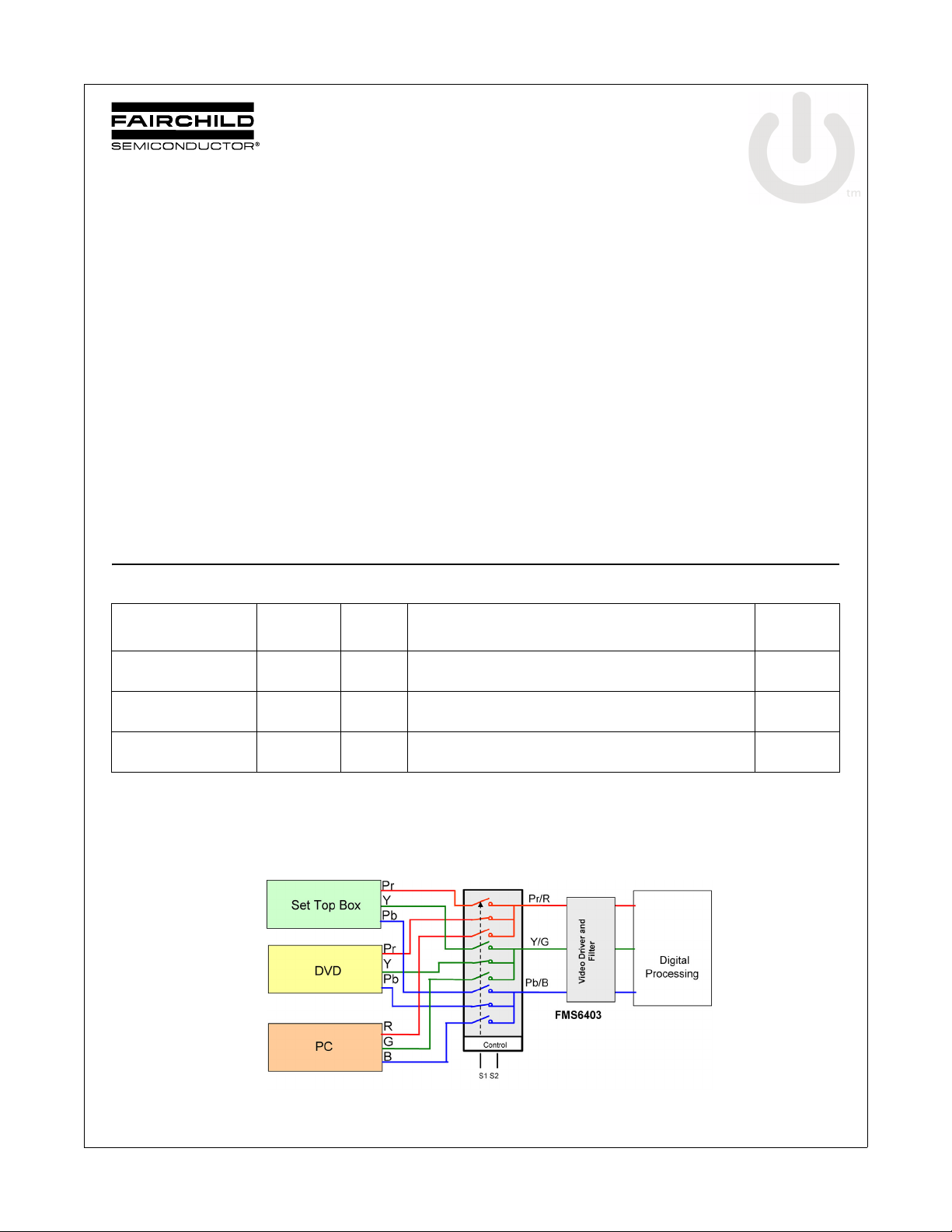
Application Diagram
© 2005 Fairchild Semiconductor Corporation www.fairchildsemi.com
FSAV433 Rev. 1.4.1

Analog Symbol Pin Descriptions
Pin Name Description
S1, S
2
ABus A
B1–B
3
Truth Table
FSAV433 High-Bandwicth (550MHz) Three-Channel 3:1 Video Switch
Select Input
Bus B
Connection Diagrams
1B
1B
1B
GND
2B
1
1
2
2
3
3
4
5
1
20
19
18
17
16
V
cc
S
1
S
2
1A
GND
S
1
S
2
Function
Low Low Disconnect
Low High A = B
High Low A = B
High High A = B
1
2
3
2B
2B
GND
3B
3B
6
2
7
3
8
9
1
10
2
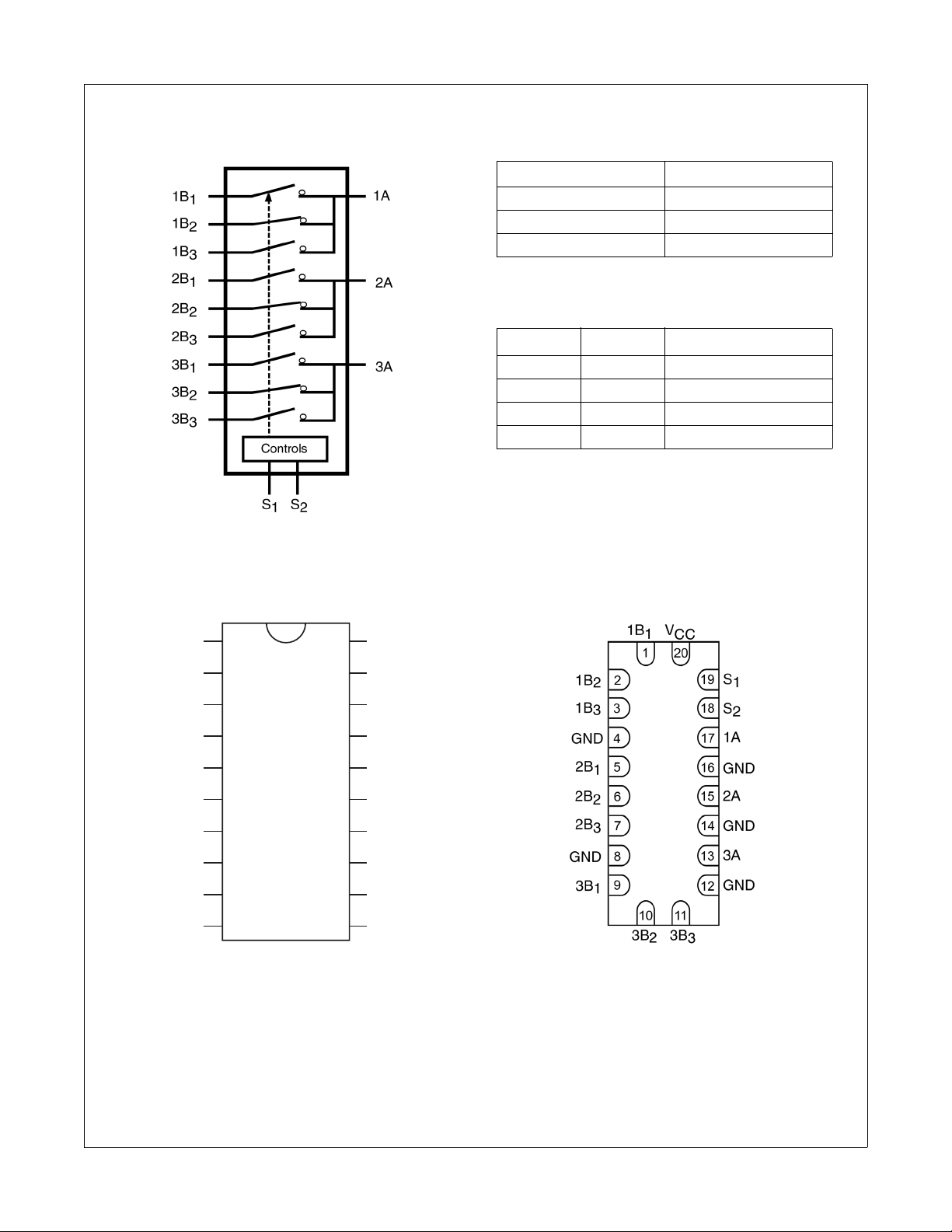
Figure 1. Pin Assignments for TSSOP
(Top Through View)
© 2005 Fairchild Semiconductor Corporation www.fairchildsemi.com
FSAV433 Rev. 1.4.1 2
15
14
13
12
11
2A
GND
3A
GND
3B
3
Figure 2. Pad Assignments for DQFN
(Top Through View)

Absolute Maximum Ratings
The “Absolute Maximum Ratings” are those values beyond which the safety of the device cannot be guaranteed. The
device should not be operated at these limits. The parametric values defined in the Electrical Characteristics tables are
not guaranteed at the absolute maximum ratings. The “Recommended Operating Conditions” table defines the conditions for actual device operation
FSAV433 High-Bandwicth (550MHz) Three-Channel 3:1 Video Switch
Symbol
V
CC
V
S
V
IN
l
IK
I
OUT
I
CC/IGND
T
STG
Parameter
Supply Voltage -0.5 +4.6 V
DC Switch Voltage -0.5V to VCC +0.05
DC Input Voltage
DC Input Diode Current VIN < 0V -50 mA
DC Output Sink Current 100 mA
DC VCC/GND Current ±100 mA
Storage Temperature Range -65 +150 °C
(2)
Min. Max. Units
-0.5 to +4.6 V
ESD Human Body Model 7 kV
Notes:
2. The input and output negative voltage ratings may be exceeded if the input and output diode current ratings are
observed.
Recommended Operating Conditions
Symbol
V
CC
V
IN
T
A
Parameter
Power Supply Operating 2.3 3.6 V
Input Voltage 0V V
Free Air Operating Temperature −40 +85 °C
(3)
Min. Max. Units
CC
Notes:
3. Unused control inputs must be held HIGH or LOW. They may not float.
© 2005 Fairchild Semiconductor Corporation www.fairchildsemi.com
FSAV433 Rev. 1.4.1 3

DC Electrical Characteristics
Typical values are at TA = +25°C unless otherwise specified.
Symbol Parameter Conditions
Analog Signal Range 0 2.0 V
V
V
V
I
OFF
R
I
CC
I
CCT
I
ON
Clamp Diode Voltage IIN = −18 mA 3.0 -1.2 V
IK
HIGH Level Input Voltage 2.3 1.8
IH
LOW Level Input Voltage 2.3 0.7
IL
Input Leakage Current 0 ≤ VIN ≤ 3.6V 3.6 ±1.0 µA
I
OFF-STATE Leakage Current 0 ≤ A, B ≤ VCC, See Figure 7 3.6 ±1.0 µA
Switch On Resistance
(4)
VIN = 1.0V 2.3 9.0 13.0 Ω
= 13 mA, See Figure 6 3.0 6.5 9.0 Ω
I
ON
= 2.0V 2.3 10.0 15.0 Ω
V
IN
= 26 mA, See Figure 6 3.0 6.5 9.0 Ω
I
ON
Quiescent Supply Current VIN = VCC or GND, I
Increase in I
Input
per Control
CC
One Control Input at 3.0V 3.6 10.0 µA
Other Inputs at V
T
= −40 °C to +85
V
(V)
= 0 3.6 1.0 µA
OUT
or GND
CC
A
CC
Min. Typ. Max.
°C
FSAV433 High-Bandwicth (550MHz) Three-Channel 3:1 Video Switch
Units
V3.0 - 3.6 2.0
V3.0 - 3.6 0.8
Notes:
4. Measured by the voltage drop between A and B pins at the indicated current through the switch. On resistance is
determined by the lower of the voltages on the two (A or B) pins.
© 2005 Fairchild Semiconductor Corporation www.fairchildsemi.com
FSAV433 Rev. 1.4.1 4
