Fairchild FSAV332 service manual

FSAV332
Quad Video Switch wit h Individual En ables
FSAV332 Quad Video Switch with Individual Enables
April 2004
Revised July 2005
General Description
The Fairchild video switch FSAV332 is a quad high speed
video switch. Low On Resistance a llows inputs to be connected to outputs without adding propagation delay or generating additional ground bounce noise.
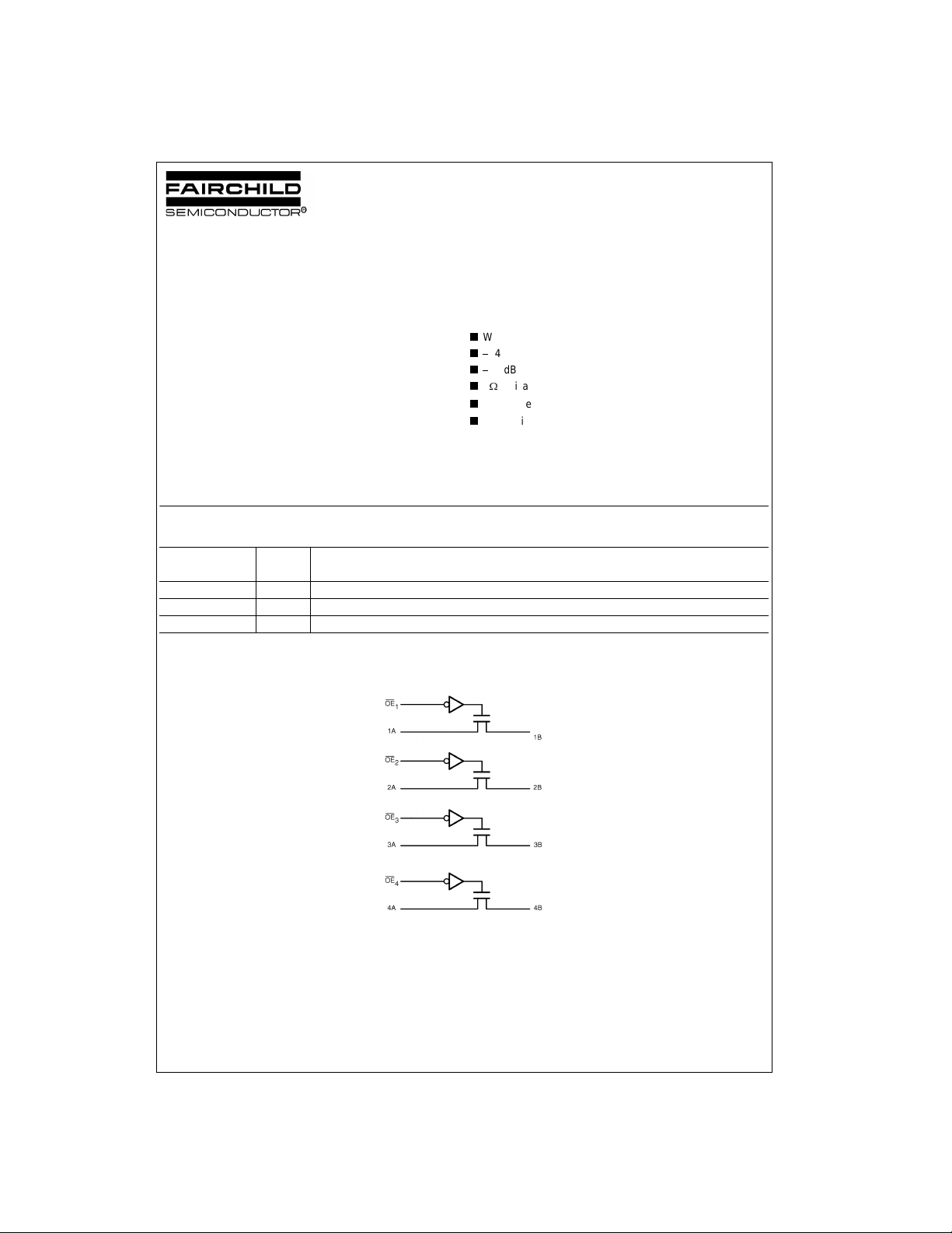
The device is o rganized as four 1-bit switches wi th separate output enable (OE) pins. Whe n OE is LOW, the switch
is ON and Port A is connected to Port B. When OE is
HIGH, the switch is OPEN and a HIGH-Impedance state
exists between the two ports.
Features
O
Wide bandwidth: 368 MHz
O
84 dB non adjacent channel crosstalk at 10MHz
O
49 dB Off Isolation at 10MHz
O3:
typical On Resistance (RON)
O
Low power consumption (3uA maximum)
O
Control input: TTL compatible
Applications
• Y/C video or CVBS video switch in LCD, plasma, and
projector displays
Ordering Code:
Order Package
Number Number
FSAV332QSC MQA16A 16-Lead Quarter Size Small Outline Package (QSOP), JEDEC MO-137, 0.150" Wide
FSAV332MTC MTC14 14-Lead Thin Shrink Small Outline Package (TSSOP), JEDEC MO-153, 4.4mm Wide
FSAV332MTC_NL MTC14 Pb-Free 14-Lead Thin Shrink Small Outline Package (TSSOP), JEDEC MO-153, 4.4mm Wide
Devices also availab l e in Tape and Reel. Specify by appending the suffix let t er “X” to the ordering code.
Pb-Free package per JEDEC J-STD-020B.
Package Description
Logic Diagram
© 2005 Fairchild Semiconductor Corporation DS500803 www.fairchildsemi.com

Connection Diagrams
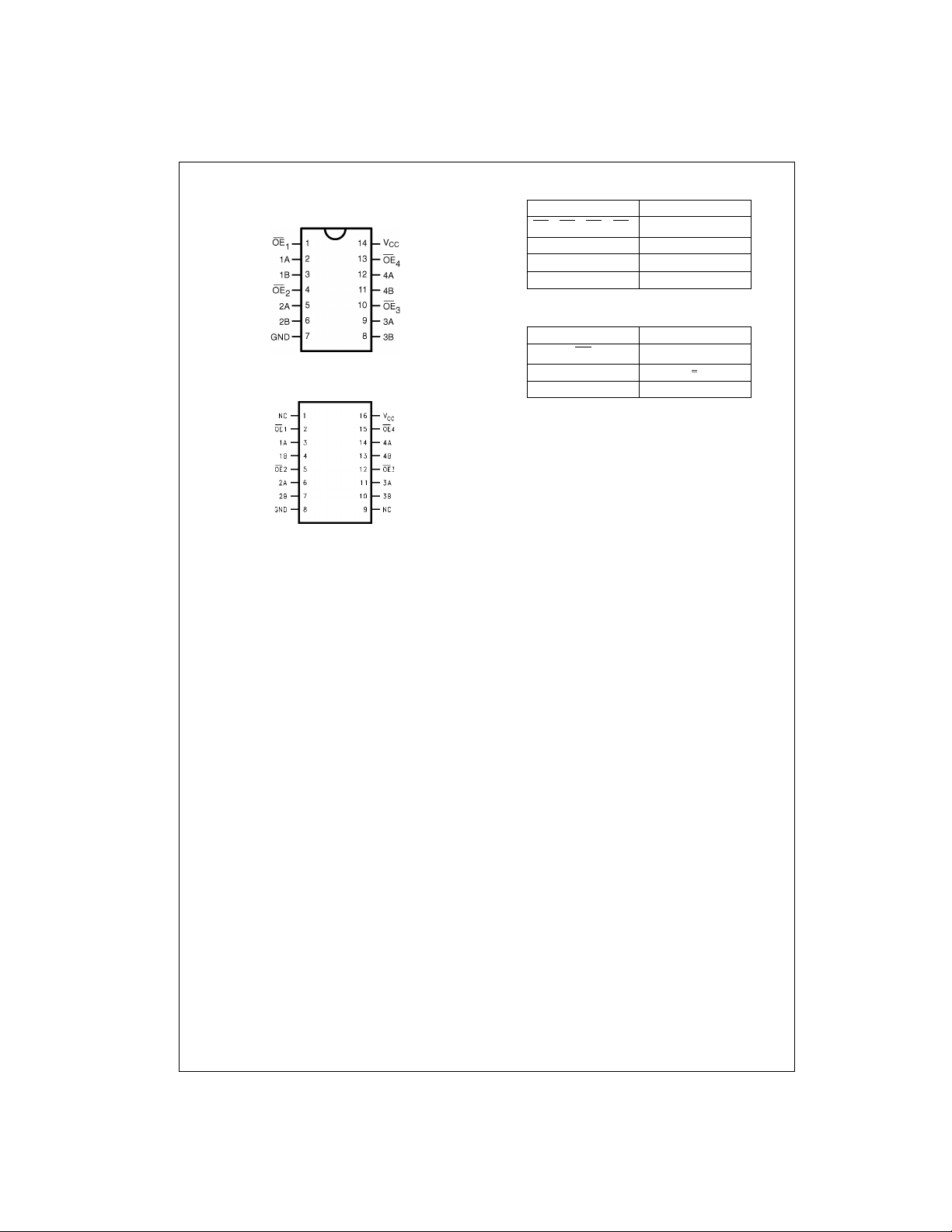
Pin Assignment for TSSOP
FSAV332
Pin Assignment for QSOP
Pin Descriptions
Pin Name Description
OE
, OE2, OE3, OE4Bus Switch Enables
1
1A, 2A, 3A, 4A Bus A
1B, 2B, 3B, 4B Bus B
NC Not Connected
Truth Table
Inputs Inputs/Outputs
OE
LA
HZ
A,B
B
www.fairchildsemi.com 2

Absolute Maximum Ratings(Note 1) Recommended Operating
Supply Voltage (VCC)
DC Switch Voltage (V
DC Input Voltage (V
S
) (Note 2)
IN
DC Input Diode Current
) (Note 2)
0.5V to 7.0V
0.5V to VCC 0.5V
0.5V to 7.0V
50 mA
DC Output Current 128 mA
Storage Temperature Range (T
STG
)
65q
C to 150qC
ESD (Human Body Model) 4000V
Conditions
Supply Voltage (V
Control Input Voltage 0V to V
Switch Input Voltage 0V to V
Operating Temperature
Thermal Resistance
(TSSOP) 115
(QSOP) 127
Note 1: The “Absolute Maximum Ratings” are those value s beyond which
the safety of the device cannot be guaranteed. The device should not be
operated at these lim its. The parametric values defin ed in the Electrical
Characteristics tables are not guaranteed at the absolute maximum rating.
The “Recomm ended O peratin g Con ditions ” table will defin e the condition s
for actual device operation.
Note 2: The input and output negative voltage ratings may be exceeded if
the input and ou t put diode current ratings are obser v ed.
Note 3: Unused control inputs m ust b e held H IGH o r LOW. They may n ot
float.
(Note 3)
) 4.75V to 5.25V
CC
40q
CC
CC
C to 85qC
q
C/W
q
C/W
FSAV332
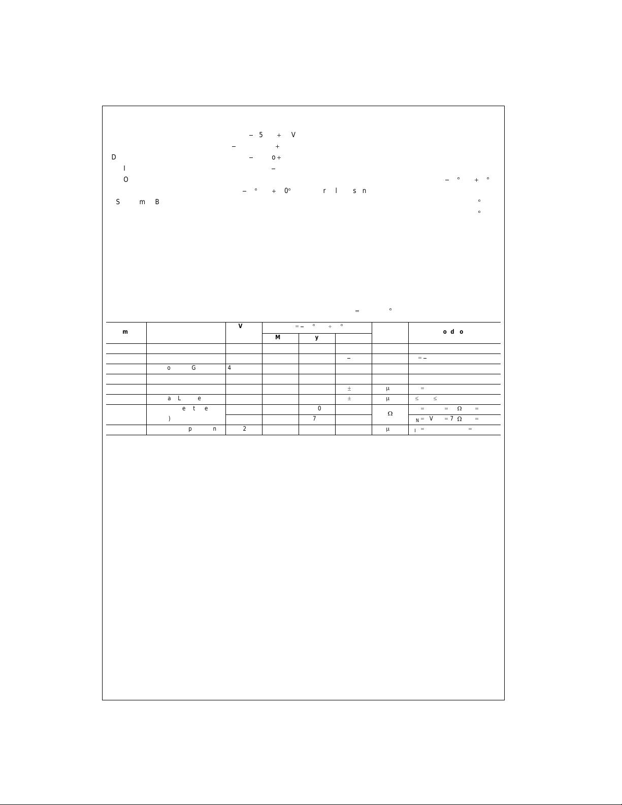
DC Electrical Characteristics All typical values are for V
V
Symbol Parameter
V
ANALOG
V
IK
V
IH
V
IL
I
IN
I
OZ
R
ON
I
CC
Note 4: Measured by the voltage drop between A and B pins at the indicated cu rrent through the switc h. On Resistance is determ ined by the lower of the
voltages on the two (A or B Ports).
Analog Signal Range 4.75 to 5.25 0 2.0 V
Clamp Diode Voltage 4.75
Input Voltage HIGH 4.75 to 5.25 2.0 V
Input Voltage LOW 4.75 to 5.25 0.8 V
Control Input Leakage 5.25
OFF State Leakage Current 5.25
Switch On Resistance 4.75 3.0 7.0
(Note 4) 4.75 7.0 10.0 V
Quiescent Supply Current 5.25 3.0
CC
(V) Min Typ Max
TA 40 qC to 85 qC
5V @ 25qC unless otherwise specified.
CC
Units Conditions
1.2 V IIN 18 mA
r
1.0
r
1.0
P
AVIN 0V to V
P
A0 d A, B d V
VIN 1V, RL 75:, ION 13 mA
:
P
2V, RL 75:, ION 26 mA
IN
AVIN 0V VCC or I
CC
CC
OUT
0
3 www.fairchildsemi.com
 Loading...