

September 2008
NC7SB3157, FSA3157
Low-Voltage SPDT Analog Switch or 2:1Multiplexer /
De-multiplexer Bus Switch
NC7SB3157, FSA3157 — Low-Voltage SPDT Analog Switch or 2:1 Multiplexer / De-multiplexer Bus Switch
Features
■ Useful in Both Analog and Digital Applications
■ Space-Saving, SC70 6-Lead Surface Mount Package
■ Ultra-Small, MicroPak™ Leadless Package
■ Low On Resistance: <10Ω on Typical at 3.3V V
■ Broad V
■ Rail-to-Rail Signal Handling
■ Power-Down, High-Impedance Control Input
■ Over-Voltage Tolerance of Control Input to 7.0V
■ Break-Before-Make Enable Circuitry
■ 250MHz, 3dB Bandwidth
Operating Range: 1.65V to 5.5V
CC
CC
Description
The NC7SB3157 / FSA3157 is a high-performance, single-pole / double-throw (SPDT) analog switch or 2:1 multiplexer / de-multiplexer bus switch.
The device is fabricated with advanced sub-micron
CMOS technology to achieve high-speed enable and
disable times and low on resistance. The break-beforemake select circuitry prevents disruption of signals on
the B Port due to both switches temporarily being
enabled during select pin switching. The device is specified to operate over the 1.65 to 5.5V V
range. The control input tolerates voltages up to 5.5V,
independent of the VCC operating range.
Ordering Information
Top
Part Number
NC7SB3157P6X B7A RoHS 6-Lead, SC70, EIAJ SC88, 1.25mm Wide Package
NC7SB3157L6X BB RoHS 6-Lead, MicroPak 1.0mm Wide Package
FSA3157P6X B7A RoHS 6-Lead, SC70, EIAJ SC88, 1.25mm Wide Package
FSA3157L6X BB RoHS 6-Lead, MicroPak 1.0mm Wide Package
Mark Eco Status Package Description
operating
CC
Packing
Method
3000 Units on
Tape and Reel
5000 Units on
Tape and Reel
3000 Units on
Tape and Reel
5000 Units on
Tape and Reel
For Fairchild’s definition of “green” Eco Status, please visit: http://www.fairchildsemi.com/company/green/rohs_green.html.
MicroPak™ is a trademark of Fairchild Semiconductor Corporation.
©2006 Fairchild Semiconductor Corporation www.fairchildsemi.com
NC7SB3157, FSA3157 Rev. 1.0.3
NC7SB3157, FSA3157 — Low-Voltage SPDT Analog Switch or 2:1 Multiplexer / De-multiplexer Bus Switch
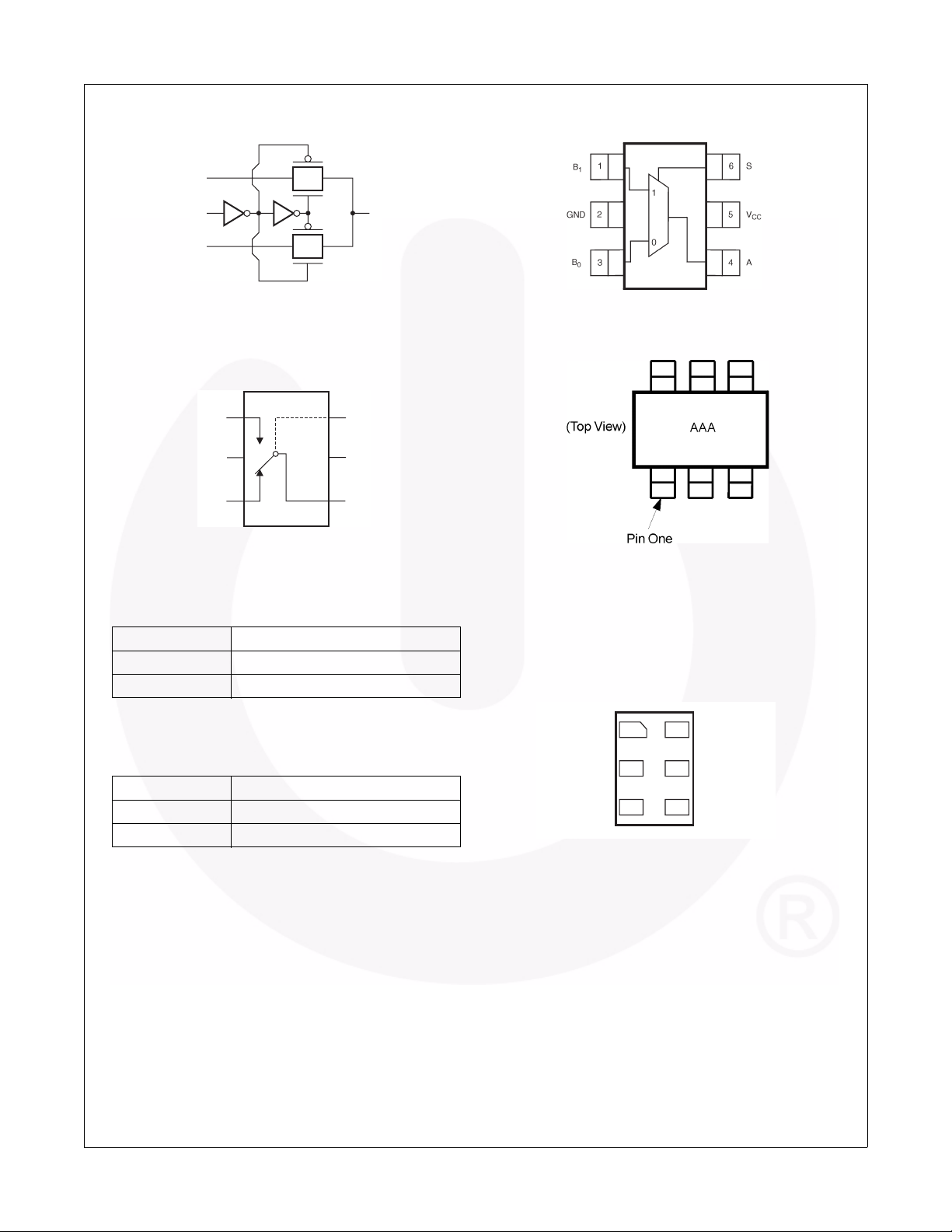
Logic Symbol
B
1
S
B
0
Figure 1. Logic Symbol
Analog Symbol
B
1
GND
B
0
Connection Diagrams
A
2. Pin Assignments SC70
S
V
CC
A
Figure 3. Analog Symbol
Function Table
Input (S) Function
Logic Level Low B0 Connected to A
Logic Level High B
Connected to A
1
Pin Descriptions
Pin Names Description
A, B0, B
1
S Control Input
Data Ports
Figure 4. Pin One Orientation
Note:
Orientation of top mark determines pin one location.
Read the top product code mark left to right and pin one
is the lower left pin (see Figure 4).
1
B
1
2
GND
34
B
0
S
6
5
V
CC
A
Figure 5. Pad Assignments for MicroPak™
© 2006 Fairchild Semiconductor Corporation www.fairchildsemi.com
NC7SB3157, FSA3157 Rev. 1.0.3 2
Absolute Maximum Ratings
Stresses exceeding the absolute maximum ratings may damage the device. The device may not function or be operable above the recommended operating conditions and stressing the parts to these levels is not recommended. In addition, extended exposure to stresses above the recommended operating conditions may affect device reliability. The
absolute maximum ratings are stress ratings only.
Symbol Parameter Min. Max. Unit
V
CC
V
S
V
IN
I
IK
I
OUT
I
CC/IGND
T
STG
T
J
T
L
P
D
ESD Human Body Model, JESD22-A114 4000 V
Note:
1. The input and output negative voltage ratings may be exceeded if the input and output diode current ratings are
observed.
Supply Voltage –0.5 +7.0 V
DC Switch Voltage
DC Input Voltage
(1)
(1)
DC Input Diode Current at VIN < 0V –50 mA
DC Output Current 128 mA
DC VCC or Ground Current ±100 mA
Storage Temperature Range –65 +150 °C
Junction Temperature Under Bias +150 °C
Junction Lead Temperature (Soldering, 10 seconds) +260 °C
Power Dissipation at +85°C 180 mW
–0.5 VCC +0.5 V
–0.5 +7.0 V
NC7SB3157, FSA3157 — Low-Voltage SPDT Analog Switch or 2:1 Multiplexer / De-multiplexer Bus Switch
Recommended Operating Conditions
The Recommended Operating Conditions table defines the conditions for actual device operation. Recommended
operating conditions are specified to ensure optimal performance to the datasheet specifications. Fairchild does not
recommend exceeding them or designing to absolute maximum ratings.
Symbol Parameter Min. Max. Unit
V
CC
V
IN
V
IN
V
OUT
T
A
tr, t
θ
JA
Note:
2. Control input must be held HIGH or LOW; it must not float.
Supply Voltage Operating 1.65 5.50 V
(2)
(2)
(2)
0 V
0 V
0 V
CC
CC
CC
Control Input Voltage
Switch Input Voltage
Output Voltage
Operating Temperature –40 +85 °C
Input Rise and Fall Time
f
Control Input
= 2.3V–3.6V
V
CC
Control Input
= 4.5V–5.5V
V
CC
0 10 ns/V
0 5 ns/V
Thermal Resistance, SC70 270 °C/W
V
V
V
© 2006 Fairchild Semiconductor Corporation www.fairchildsemi.com
NC7SB3157, FSA3157 Rev. 1.0.3 3
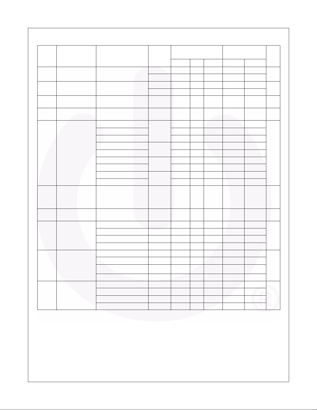
DC Electrical Characteristics
= –40°C to
T
= +25°C
T
Symbol Parameter Conditions V
CC
(V)
A
Min. Typ. Max. Min. Max.
V
V
I
OFF
R
I
R
RANGE
ΔR
R
High Level
IH
Input Voltage
Low Level
IL
Input Voltage
Input Leakage
I
IN
Current
Off State Leakage
Current
Switch On
ON
Resistance
Quiescent Supply
Current;
CC
All Channels On or
Off
Analog Signal
Range
On Resistance Over
Signal Range
On Resistance
Match Between-
ON
Channels
On Resistance
flat
Flatness
(3)
(3, 4, 5)
(3, 4, 6)
0 ≤ V
≤ 5.5V 0 – 5.5 ±0.05 ±0.1 ±1 µA
IN
0 ≤ A, B ≤ V
CC
VIN = 0V, IO = 30mA 4.5 3.0 7.0 7.0
V
= 2.4V, IO = –30mA 5.0 12.0 12.0
IN
= 4.5V, IO = –30mA 7.0 15.0 15.0
V
IN
= 0V, IO = 24mA 3.0 4.0 9.0 9.0
V
IN
= 3V, IO = –24mA 10.0 20.0 20.0
V
IN
= 0V, IO = 8mA 2.3 5.0 12.0 12.0
V
IN
= 2.3V, IO = –8mA 13.0 30.0 30.0
V
IN
= 0V, IO = 4mA 1.65 6.5 20.0 20.0
V
IN
= 1.65V, IO = –4mA 17.0 50.0 50.0
V
IN
V
= VCC or GND I
IN
OUT
IA = –30mA, 0 ≤ VBn ≤ V
(3, 7)
= –8mA, 0 ≤ VBn ≤ V
I
A
= –4mA, 0 ≤ VBn ≤ V
I
A
= –24mA, 0 ≤ VBn ≤ V
I
A
IA = –30mA, VBn = 3.15 4.5 0.15
= –24mA, VBn 2.1 3.0 0.2
I
A
I
= –8mA, VBn = 1.6
A
= –4mA, VBn = 1.15 1.65 0.50
I
A
IA = –30mA, 0 ≤ V
= –24mA, 0 ≤ V
I
A
= –8mA, 0 ≤ V
I
A
I
= –4mA, 0 ≤ V
A
Bn
Bn
Bn
Bn
≤ V
≤ V
1.65 – 1.95 0.75 V
2.3 – 5.5 0.7 V
1.65 – 1.95 0.25 V
2.3 – 5.5 0.3 V
CC
CC
CC
CC
1.65 – 5.5 ±0.05 ±0.1 ±1 µA
= 0 5.5 1 10 µA
≤ V
≤ V
CC
CC
CC
CC
V
CC
4.5 25.0
CC
3.0 50.0
CC
2.3 100
1.65 300
2.3
5.0 6.0
CC
3.3 12.0
CC
2.5 28.0
1.8 125
0VCC0VCCV
0.5
Notes:
3. Measured by the voltage drop between A and B pins at the indicated current through the switch. On resistance is
determined by the lower of the voltages on the two (A or B Ports).
4. Parameter is characterized, but not tested in production.
5. ΔR
= RON max – RON minimum measured at identical VCC, temperature, and voltage levels.
ON
6. Flatness is defined as the difference between the maximum and minimum value of on resistance over the specified
range of conditions.
7. Guaranteed by design.
A
0.75 V
0.7 V
+85°C
CC
CC
0.25 V
0.3 V
CC
CC
Units
V
V
Ω
Ω
Ω
Ω
NC7SB3157, FSA3157 — Low-Voltage SPDT Analog Switch or 2:1 Multiplexer / De-multiplexer Bus Switch
© 2006 Fairchild Semiconductor Corporation www.fairchildsemi.com
NC7SB3157, FSA3157 Rev. 1.0.2 4

AC Electrical Characteristics
= –40°C to
T
A
+85°C
ns
ns
Figure
Number
Figure 12
Figure 13
Figure 12
Figure 13
Units
Figure 12
ns
Figure 13
ns Figure 14
pC Figure 15
Symbol Parameter Conditions
V
CC
(V)
TA = +25°C
Min. Typ. Max. Min. Max.
1.65 – 1.95 3.5 3.5
t
t
PHL
PLH
,
Propagation Delay
Bus-to-Bus
(8)
VI = OPEN
2.3 – 2.7 1.2 1.2
3.0 – 3.6 0.8 0.8
4.5 – 5.5 0.3 0.3
1.65 – 1.95 7.0 23.0 7.0 24.0
t
t
PZL
PZH
Output Enable Time
,
Turn-On Time
(A to B
n
V
= 2 x VCC for t
I
)
VI = 0V for t
PZL
PZH
2.3 – 2.7 3.5 13.0 3.5 14.0
3.0 – 3.6 2.5 6.9 2.5 7.6
4.5 – 5.5 1.7 5.2 1.7 5.7
1.65 – 1.95 3.0 12.5 3.0 13.0
t
t
PLZ
PHZ
Output Disable Time
,
Turn-Off Time
(A Port to B Port)
V
= 2 x V
I
VI = 0V for t
CC
for t
PHZ
PLZ
2.3 – 2.7 2.0 7.0 2.0 7.5
3.0 – 3.6 1.5 5.0 1.5 5.3
4.5 – 5.5 0.8 3.5 0.8 3.8
1.65 –1.95 0.5 0.5
t
B-M
Break-Before-Make
(9)
Time
2.3 – 2.7 0.5 0.5
3.0 – 3.6 0.5 0.5
4.5 – 5.5 0.5 0.5
Q Charge Injection
OIRR Off Isolation
(9)
(10)
Xtalk Crosstalk R
BW –3dB Bandwidth R
THD
Total Harmonic
Distortion
(9)
CL = 0.1nF, V
= 0Ω 3.3 3.0
R
GEN
RL = 50Ω, f = 10MHz 1.65 – 5.5 –57.0 dB Figure 16
= 50Ω, f = 10MHz 1.65 – 5.5 –54.0 dB Figure 17
L
= 50Ω 1.65 – 5.5 250 MHz Figure 20
L
RL = 600Ω, 0.5 VPP,
f = 600 Hz to 20 KHz
= 0V, 5.0 7.0
GEN
5.0 .011 %
Notes:
8. This parameter is guaranteed by design but not tested. The bus switch contributes no propagation delay other than
the RC delay of the on resistance of the switch and the 50pF load capacitance, when driven by an ideal voltage
source (zero output impedance).
9. Guaranteed by design.
10. Off Isolation = 20 log
[VA / VBn].
10
NC7SB3157, FSA3157 — Low-Voltage SPDT Analog Switch or 2:1 Multiplexer / De-multiplexer Bus Switch
Capacitance
TA = +25°C, f = 1MHz. Capacitance is characterized, but not tested in production.
Symbol Parameter Conditions Typ. Max. Units
C
Control Pin Input Capacitance VCC = 0V 2.3 pF
IN
C
C
IOA-ON
© 2006 Fairchild Semiconductor Corporation www.fairchildsemi.com
NC7SB3157, FSA3157 Rev. 1.0.2 5
B Port Off Capacitance VCC = 5.0V 6.5 pF Figure 18
IO-B
A Port Capacitance When Switch Is Enabled VCC = 5.0V 18.5 pF Figure 19
Figure
Number

Typical Characteristics
NC7SB3157, FSA3157 — Low-Voltage SPDT Analog Switch or 2:1 Multiplexer / De-multiplexer Bus Switch
0
-10
VCC = 1.65V
-20
-30
-40
-50
-60
-70
-80
-90
Off Isolation (dB)
-100
-110
-120
1 10 100 1000
Frequency (MHz)
0
-10
VCC = 5.5V
-20
-30
-40
-50
-60
-70
-80
-90
Off Isolation (dB)
-100
-110
-120
1 10 100 1000
Frequency (MHz)
Figure 6. Off Isolation, VCC = 1.65V Figure 7. Off Isolation, VCC = 5.5V
0
-10
VCC = 1.65V
-20
-30
-40
-50
-60
-70
-80
Crosstalk (dB)
-90
-100
-110
-120
1 10 100 1000
Frequency (MHz)
0
-10
VCC = 5.5V
-20
-30
-40
-50
-60
-70
-80
Crosstalk (dB)
-90
-100
-110
-120
1 10 100 1000
Frequency (MHz)
Figure 8. Crosstalk, VCC = 1.65V Figure 9. Crosstalk, VCC = 5.5V
0
-1
-2
-3
-4
-5
Gain (dB)
-6
CL = 0pF
-7
-8
= 1.65V
V
CC
1 10 100 1000
Frequency (MHz)
0
-1
-2
-3
-4
-5
Gain (dB)
-6
CL = 0pF
-7
-8
= 5.5V
V
CC
1 10 100 1000
Frequency (MHz)
Figure 10. Bandwidth, VCC = 1.65V Figure 11. Bandwidth, VCC = 5.5V
© 2006 Fairchild Semiconductor Corporation www.fairchildsemi.com
NC7SB3157, FSA3157 Rev. 1.0.2 6

AC Loading and Waveforms
tr = 2.5ns
Switch
Input
Output
90% 90%
50%
t
t
PLH
W
50%
t
PHL
V
I
FROM
RU
OUTPUT
UNDER
TEST
C
L
RD
Notes:
Input driven by 50Ω source terminated in 50Ω
includes load and stray capacitance
C
L
Input PRR = 1.0 MHz; t
= 500 ns
W
Figure 12. AC Test Circuit
= 2.5ns tr = 2.5ns
t
r
90%
t
10%10%
= 2.5ns
r
50%50%
V
CC
GND
V
OH
V
OL
Control
Input
Output
Output
10%
t
t
50%
PZL
PZH
50%
50%
90%
50%
10%
t
PLZ
VOL+0.3V
V
OL
t
PHZ
V
OH
VOH–0.3V
V
CC
GND
NC7SB3157, FSA3157 — Low-Voltage SPDT Analog Switch or 2:1 Multiplexer / De-multiplexer Bus Switch
V
TRI
V
TRI
Figure 13. AC Waveforms
B
V
Logic
Input
IN
0
A
B
1
R
S
L
V
OUT
C
L
Logic
Input
V
OUT
0.9 x V
OUT
t
D
Figure 14. Break-Before-Make Interval Timing
© 2006 Fairchild Semiconductor Corporation www.fairchildsemi.com
NC7SB3157, FSA3157 Rev. 1.0.3 7

AC Loading and Waveforms (continued)
NC7SB3157, FSA3157 — Low-Voltage SPDT Analog Switch or 2:1 Multiplexer / De-multiplexer Bus Switch
V
GE
Logic
Input
Analyzer
R
GEN
B
A
N
S
10nF
V
CC
A
50Ω
S
B
N
50Ω
GND
Figure 16. Off Isolation
10nF
Logic
V
R
1MΩ 100pF
C
L
L
OUT
Input
V
Figure 15. Charge Injection Test
Signal
Logic Input
0V or V
IH
Generator
0dBm
OUT
Analyzer
OFF OFFON
Q = (ΔV
OUT
)(CL)
10nF
V
CC
B
0
B
1
GND
50Ω
Figure 17. Crosstalk
10nF
ΔV
OUT
A
50Ω
S
V
CC
A
Capacitance
Meter
f = 1MHz
B
S
N
GND
Figure 18. Channel Off Capacitance
Signal
Generator
0dBm
Logic Input
0V or V
CC
Logic Input
0V or V
CC
Figure 20. Bandwidth
10nF
B
N
S
V
GND
CC
Capacitance
Meter
V
CC
A
f = 1MHz
S
B
N
GND
Figure 19. Channel On Capacitance
A
50Ω
Logic Input
0V or V
CC
© 2006 Fairchild Semiconductor Corporation www.fairchildsemi.com
NC7SB3157, FSA3157 Rev. 1.0.3 8

Physical Dimensions
NC7SB3157, FSA3157 — Low-Voltage SPDT Analog Switch or 2:1 Multiplexer / De-multiplexer Bus Switch
Figure 21. 6-Lead, SC70, EIAJ SC88, 1.25mm Wide Package
Note: click here for tape and reel specifcations, available at:
http://www.fairchildsemi.com/products/analog/pdf/sc70-6_tr.pdf
Package drawings are provided as a service to customers considering Fairchild components. Drawings may change in any manner
without notice. Please note the revision and/or date on the drawing and contact a Fairchild Semiconductor representative to verify or
obtain the most recent revision. Package specifications do not expand the terms of Fairchild’s worldwide terms and conditions,
specifically the warranty therein, which covers Fairchild products.
Always visit Fairchild Semiconductor’s online packaging area for the most recent package drawings:
http://www.fairchildsemi.com/packaging/
© 2006 Fairchild Semiconductor Corporation www.fairchildsemi.com
NC7SB3157, FSA3157 Rev. 1.0.2 9
.

Physical Dimensions
2X
0.05
NC7SB3157, FSA3157 — Low-Voltage SPDT Analog Switch or 2:1 Multiplexer / De-multiplexer Bus Switch
C
1.45
2X
B
(1)
0.05
C
(0.49)
5X
(0.52)
1X
PIN 1
C
0.075 X 45
CHAMFER
0.05
DETAIL A
(0.05)
6X
C
0.55MAX
C
BOTTOM VIEW
TOP VIEW
1.0
0.5
1.00
A
0.05
0.00
0.05
0.25
6X
0.15
0.10 C B A
0.05 C
0.35
5X
0.25
0.40
5X
0.30
(0.13)
4X
Notes:
1. CONFORMS TO JEDEC STANDARD M0-252 VARIATION UAAD
2. DIMENSIONS ARE IN MILLIMETERS
3. DRAWING CONFORMS TO ASME Y14.5M-1994
(0.30)
6X
RECOMMENED
LAND PATTERN
0.10
6X
0.00
0.40
0.30
DETAIL A
PIN 1 TERMINAL
(0.75)
0.45
0.35
MAC06AREVC
6-Lead, MicroPak™ 1.0mm Wide Package
Note: click here for tape and reel specifcations, available at:
http://www.fairchildsemi.com/products/logic/pdf/micropak_tr.pdf
Package drawings are provided as a service to customers considering Fairchild components. Drawings may change in any manner
without notice. Please note the revision and/or date on the drawing and contact a Fairchild Semiconductor representative to verify or
obtain the most recent revision. Package specifications do not expand the terms of Fairchild’s worldwide terms and conditions,
specifically the warranty therein, which covers Fairchild products.
Always visit Fairchild Semiconductor’s online packaging area for the most recent package drawings:
http://www.fairchildsemi.com/packaging/.
© 2006 Fairchild Semiconductor Corporation www.fairchildsemi.com
NC7SB3157, FSA3157 Rev. 1.0.2 10

NC7SB3157, FSA3157 — Low-Voltage SPDT Analog Switch or 2:1 Multiplexer / De-multiplexer Bus Switch
© 2006 Fairchild Semiconductor Corporation www.fairchildsemi.com
NC7SB3157, FSA3157 Rev. 1.0.3 11
 Loading...