

现货库存、技术资料、百科信息、热点资讯,精彩尽在鼎好!
May 2000
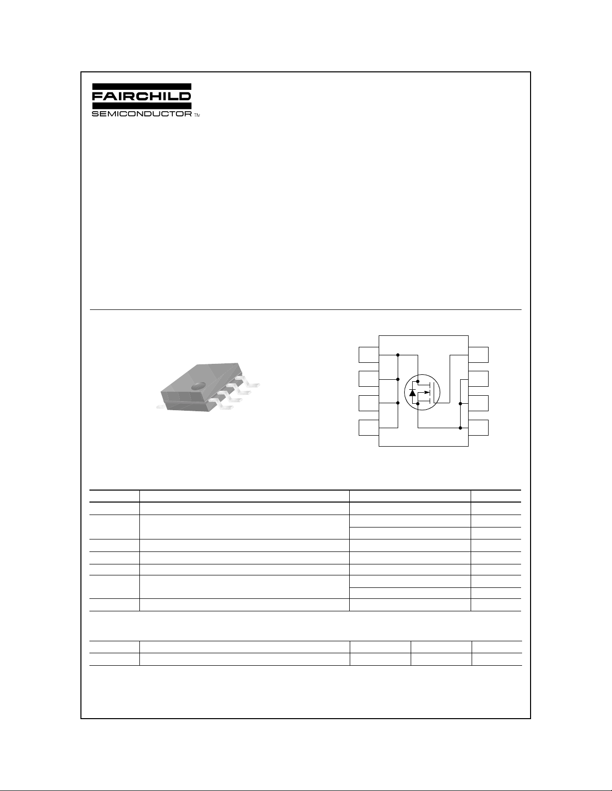
FQS4410
FQS4410
Single N-Channel, Logic Level, Power MOSFET
General Description
These N-Channel enhancement mode power field effect
transistors are produced using Fairchild’s proprietary,
planar stripe, DMOS technology.
This advanced technology has been especially tailored to
minimize on-state resistance, provide superior switching
performance, and withstand high energy pulse in the
avalanche and commutation mode. These devices are well
suited for low voltage applications such as DC/DC
converters, high efficiency switching for power
management in portable and battery operated products.
Features
• 10A, 30V, R
• Low gate charge ( typical 21 nC)
• Low Crss ( typical 145 pF)
• Fast switching
• Improved dv/dt capability
• 175°C maximum junction temperature rating
= 0.0135Ω @VGS = 10 V
DS(on)
8
7
6
QFET
QFET
QFETQFET
4
3
2
TM
5
Absolute Maximum Ratings T
Symbol Parameter FQS4410 Units
V
DSS
I
D
I
DM
V
GSS
dv/dt Peak Diode Recovery dv/dt
P
D
T
, T
J
STG
Drain-Source Voltage 30 V
Drain Current
Drain Current - Pulsed
Gate-Source Voltage ± 20 V
Power Dissipation (TC = 25°C)
Linear Derating Factor 0.02 W/°C
Operating and Storage Temperature Range -55 to +175 °C
- Continuous (T
- Continuous (T
= 25°C unless otherwise noted
C
= 25°C)
C
= 70°C)
C
(Note 1)
(Note 3)
10 A
8A
50 A
7.0 V/ns
2.5 W
1
Thermal Characteristics
Symbol Parameter Typ Max Units
R
θJA
Thermal Resistance, Junction-to-Ambient -- 50 °C/W
©2000 Fairchild Semiconductor International
Rev. A, May 2000
FQS4410
Electrical Characteristics T
= 25°C unless otherwise noted
C
Symbol Parameter Test Conditions Min Typ Max
Off Characteristics
BV
DSS
∆BV
DSS
/ ∆T
I
DSS
I
GSSF
I
GSSR
Drain-Source Breakdown Voltage
Breakdown Voltage Temperature
Coefficient
J
Zero Gate Voltage Drain Current
Gate-Body Leakage Current, Forward
Gate-Body Leakage Current, Reverse
= 0 V, ID = 250 µA
V
GS
= 250 µA, Referenced to
I
D
25°C
V
= 30 V, VGS = 0 V
DS
V
= 24 V, TC = 125°C
DS
= 20 V, VDS = 0 V
V
GS
V
= -20 V, VDS = 0 V
GS
30 -- -- V
-- 0.03 -- V/°C
-- -- 1 µA
-- -- 10 µA
-- -- 100 nA
-- -- -100 nA
On Characteristics
V
R
g
FS
GS(th)
DS(on)
Gate Threshold Voltage
Static Drain-Source
On-Resistance
Forward Transconductance
V
= VGS, ID = 250 µA
DS
= 10 V, ID = 10 A
V
GS
V
= 4.5 V, ID = 5 A
GS
= 10 V, ID = 5 A
V
DS
(Note 4)
1.0 -- 2.5 V
--
--
--
--
-- 16 -- S
Dynamic Characteristics
C
iss
C
oss
C
rss
Input Capacitance
Output Capacitance -- 590 770 pF
Reverse Transfer Capacitance -- 145 190 pF
= 25 V, VGS = 0 V,
V
DS
f = 1.0 MHz
-- 980 1280 pF
Switching Characteristics
t
d(on)
t
r
t
d(off)
t
f
Q
Q
Q
g
gs
gd
Turn-On Delay Time
Turn-On Rise Time -- 165 340 ns
Turn-Off Delay Time -- 65 140 ns
Turn-Off Fall Time -- 110 23 0 ns
Total Gate Charge
Gate-Source Charge -- 4.2 -- nC
Gate-Drain Charge -- 12 -- nC
V
= 15 V, ID = 5 A,
DD
R
= 50 Ω
G
= 24 V, ID = 10 A,
V
DS
V
GS
= 5 V
(Note 4, 5)
(Note 4, 5)
-- 30 70 ns
-- 21 28 nC
0.0135
0.02
Unit
s
Ω
Drain-Source Diode Characteristics and Maximum Ratings
I
S
I
SM
V
SD
t
rr
Q
rr
Notes:
1. Repetitive Rating : Pulse width limited by maximum junction temperature
2. L = 3mH, IAS = 10A, VDD = 15V, RG = 25 Ω, Starting TJ = 25°C
3. ISD ≤ 10A, di/dt ≤ 300A/us, VDD ≤ BV
4. Pulse Test : Pulse width ≤ 300µs, Duty cycle ≤ 2%
5. Essentially independent of operating temperature
©2000 Fairchild Semiconductor International
Maximum Continuous Drain-Source Diode Forward Current -- -- 2.3 A
Maximum Pulsed Drain-Source Diode Forward Current -- -- 50 A
= 0 V, IS = 2.3 A
Drain-Source Diode Forward Voltage
Reverse Recovery Time
Reverse Recovery Charge -- 45 -- nC
Starting TJ = 25°C
DSS,
V
GS
= 0 V, IS = 24 A,
V
GS
dI
/ dt = 100 A/µs
F
(Note 4)
-- -- 1.1 V
-- 45 -- ns
Rev. A, May 2000
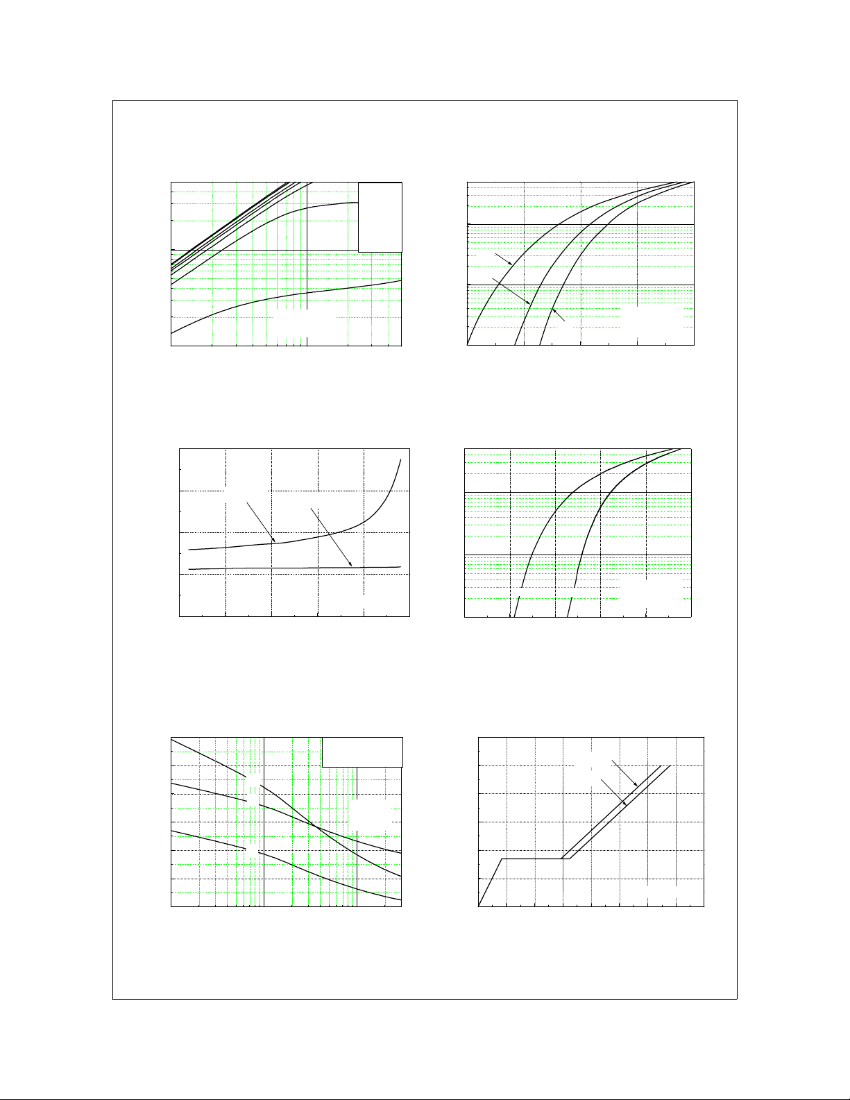
Typical Characteristics
FQS4410
1
10
, Drain Current [A]
D
I
0
10
-1
10
VDS, Drain-Source Voltage [V]
Figure 1. Output Characte ri st ic s
※
Not e :
1. 250μs Pulse Test
℃
= 25
2. T
C
0
10
V
Top : 10 .0 V
8.0 V
6.0 V
5.0 V
4.5 V
4.0 V
3.5 V
Bottom : 3.0 V
GS
1
10
℃
150
℃
25
0
10
, Drain Current [A]
D
I
-1
10
2.0 2.5 3.0 3.5 4.0
VGS, Gate-Source Voltage [V]
Figure 2. Transfer Characteristics
※
Note
1. V
= 10V
℃
-55
DS
2. 250μs Pulse Test
40
30
],
Ω
20
[m
DS(ON)
R
10
Drain-Source On-Resistance
0
0 1020304050
VGS = 4.5V
VGS = 10V
※
Note : T
J
ID, Drain Current [A]
= 25
℃
1
10
0
10
※
℃
, Reverse Drain Current [A]
DR
I
-1
10
0.2 0.4 0.6 0.8 1.0 1.2
150
℃
25
Not e :
= 0V
1. V
GS
2. 250μs Pul se Test
VSD, Source-Drain voltage [V]
Figure 3. On-Resistance Variati on vs.
Drain Current
3000
2500
2000
1500
1000
Capacitance [pF]
500
0
-1
10
VDS, Drain-Source Voltage [V]
C
iss
C
oss
C
rss
C
oss
C
iss
C
rss
0
10
Figure 5. Capacitance vs. Drai n-Source Voltage
©2000 Fairchild Semiconductor International
= Cgs + Cgd (Cds = shorted)
= Cds + C
gd
= C
gd
※
Note ;
= 0 V
1. V
GS
2. f = 1 MHz
1
10
Figure 4. Source-Drain Diode Forward Voltage
12
10
VDS = 15V
VDS = 24V
8
6
4
2
, Gate-Source Voltage [V]
GS
V
0
0 5 10 15 20 25 30 35 40
QG, Total Gate Charge [nC]
Figure 6. Gate Charge vs. Gate-Source Voltage
※
Note : I
= 10A
D
Rev. A, May 2000
 Loading...