

现货库存、技术资料、百科信息、热点资讯,精彩尽在鼎好!
FQPF5P10
100V P-Channel MOSFET
FQPF5P10
TM
QFET
General Description
These P-Channel enhancement mode power field effect
transistors are produced using Fairchild’s proprietary,
planar stripe, DMOS technology.
This advanced technology has been especially tailored to
minimize on-state resistance, provide superior switching
performance, and withstand high energy pulse in the
avalanche and commutation mode. These devices are well
suited for low voltage applications such as audio amplifier,
high efficiency switching DC/DC converters, and DC motor
control.
GSD
Absolute Maximum Ratings T
Symbol Parameter FQPF5P10 Units
V
DSS
I
D
I
DM
V
GSS
E
AS
I
AR
E
AR
dv/dt Peak Diode Recovery dv/dt
P
D
T
, T
J
STG
T
L
Drain-Source Voltage -100 V
Drain Current
Drain Current - Pulsed
Gate-Source Voltage ± 30 V
Single Pulsed Avalanche Energy
Avalanche Current
Repetitive Avalanche Energy
Power Dissipation (TC = 25°C)
Operating and Storage Temperature Range -55 to +175 °C
Maximum lead temperature for soldering purposes,
1/8" from case for 5 seconds
- Continuous (T
- Continuous (T
- Derate above 25°C 0.15 W/°C
TO-220F
FQPF Series
= 25°C unless otherwise noted
C
= 25°C)
C
= 100°C)
C
Features
• -2.9A, -100V, R
• Low gate charge ( typical 6.3 nC)
• Low Crss ( typical 18 pF)
• Fast switching
• 100% avalanche tested
• Improved dv/dt capability
• 175°C maximum junction temperature rating
G
(Note 1)
(Note 2)
(Note 1)
(Note 1)
(Note 3)
= 1.05Ω @VGS = -10 V
DS(on)
D
S
-2.9 A
-2.08 A
-11.6 A
55 mJ
-2.9 A
2.3 mJ
-6.0 V/ns
23 W
300 °C
Thermal Characteristics
Symbol Parameter Typ Max Units
R
θJC
R
θJA
©2002 Fairchild Semiconductor Corporation
Thermal Resistance, Junction-to-Case -- 6.52 °C/W
Thermal Resistance, Junction-to-Ambient -- 62.5 °C/W
Rev. B, August 2002
FQPF5P10
Electrical Characteristics T
= 25°C unless otherwise noted
C
Symbol Parameter Te st Conditions Min Typ Max Units
Off Characteristics
BV
DSS
∆BV
DSS
/ ∆T
I
DSS
I
GSSF
I
GSSR
Drain-Source Breakdown Voltage
Breakdown Voltage Temperature
Coefficient
J
Zero Gate Voltage Drain Current
Gate-Body Leakage Current, Forward
Gate-Body Leakage Current, Reverse
= 0 V, ID = -250 µA
V
GS
I
= -250 µA, Referenced to 25°C
D
V
= -100 V, VGS = 0 V
DS
V
= -80 V, TC = 150°C
DS
V
= -30 V, VDS = 0 V
GS
= 30 V, VDS = 0 V
V
GS
-100 -- -- V
-- -0.1 -- V/°C
-- -- -1 µA
-- -- -10 µA
-- -- -100 nA
-- -- 100 nA
On Characteristics
V
R
g
FS
GS(th)
DS(on)
Gate Threshold Voltage
Static Drain-Source
On-Resistance
Forward Transconductance
V
= VGS, ID = -250 µA
DS
= -10 V, ID = -1.45 A
V
GS
= -40 V, ID = -1.45 A
V
DS
(Note 4)
-2.0 -- -4.0 V
-- 0.82 1.05 Ω
-- 2.1 -- S
Dynamic Characteristics
C
iss
C
oss
C
rss
Input Capacitance
Output Capacitance -- 70 90 pF
Reverse Transfer Capacitance -- 18 25 pF
= -25 V, VGS = 0 V,
V
DS
f = 1.0 MHz
-- 190 250 pF
Switching Characteristics
t
d(on)
t
r
t
d(off)
t
f
Q
Q
Q
g
gs
gd
Turn-On Delay Time
Turn-On Rise Time -- 70 150 ns
Turn-Off Delay Time -- 12 35 ns
Turn-Off Fall Time -- 30 70 n s
Total Gate Charge
Gate-Source Charge -- 1.7 -- nC
Gate-Drain Charge -- 3.0 -- nC
= -50 V, ID = -4.5 A,
V
DD
= 25 Ω
R
G
V
= -80 V, ID = -4.5 A,
DS
V
GS
= -10 V
(Note 4, 5)
(Note 4, 5)
-- 9 30 ns
-- 6.3 8.2 nC
Drain-Source Diode Characteristics and Maximum Ratings
I
S
I
SM
V
SD
t
rr
Q
rr
Notes:
1. Repetitive Rating : Pulse width limited by maximum junction temperature
2. L = 9.8mH, IAS = -2.9A, VDD = -25V, RG = 25 Ω, Starting TJ = 25°C
3. ISD ≤ -4.5A, di/dt ≤ 300A/µs, VDD ≤ BV
4. Pulse Test : Pulse width ≤ 300µs, Duty cycle ≤ 2%
5. Essentially independent of operating temperature
©2002 Fairchild Semiconductor Corporation
Maximum Continuous Drain-Source Diode Forward Current -- -- -2.9 A
Maximum Pulsed Drain-Source Diode Forward Current -- -- -11.2 A
= 0 V, IS = -2.9 A
Drain-Source Diode Forward Voltage
Reverse Recovery Time
Reverse Recovery Charge -- 0.27 -- µC
Starting TJ = 25°C
DSS,
V
GS
= 0 V, IS = -4.5 A,
V
GS
/ dt = 100 A/µs
dI
F
-- -- -4.0 V
-- 85 -- ns
(Note 4)
Rev. B, August 2002
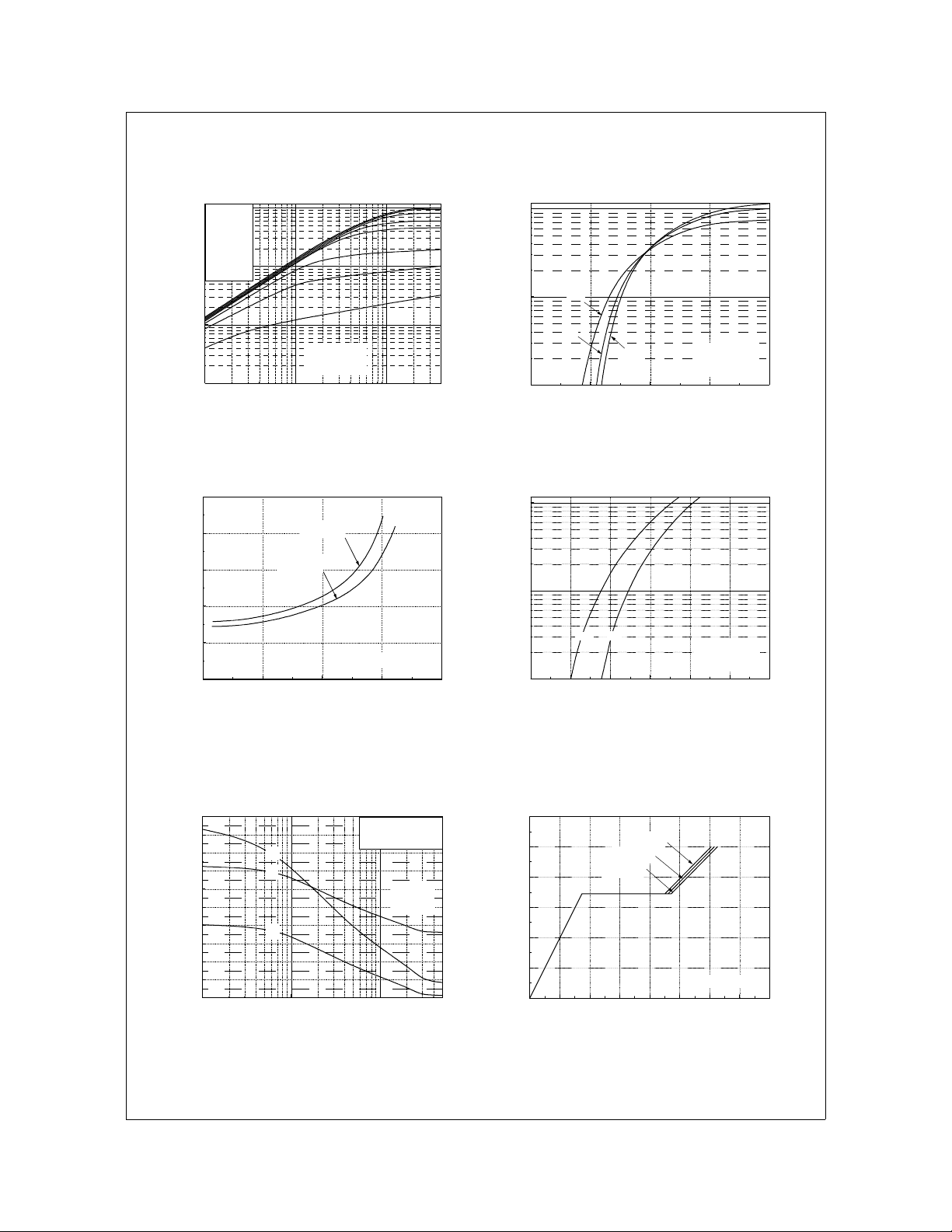
Typical Characteristics
FQPF5P10
※
Note s :
1. 250
µs Pulse Test
℃
2. T
= 25
C
0
10
1
10
, Drain Current [A]
D
-I
1
10
0
10
-1
10
-2
10
10
V
Top : -1 5 .0 V
-10 .0 V
-8.0 V
-7.0 V
-6.5 V
-5.5 V
-5.0 V
Botto m : -4.5 V
-1
GS
-VDS, Drain-Source Voltage [V]
VGS = - 10V
VGS = - 20V
※
℃
Note : T
= 25
J
2.5
2.0
],
Ω
1.5
[
DS(on)
R
1.0
Drain-Source On-Resistance
0.5
0.0
036912
-ID , Drai n Curren t [A]
1
10
0
10
, Drain Current [A]
D
-I
-1
10
246810
℃
175
℃
25
※
℃
-55
Notes :
1. V
= -40V
DS
2. 250μs Pulse Test
-VGS , Gate-Source Voltage [V]
Figure 2. Transfer CharacteristicsFigure 1. On-Region Char act er i stic s
1
10
0
10
℃
, Reve rs e D ra in Current [A ]
DR
-I
-1
10
0.0 0.5 1.0 1.5 2.0 2.5 3.0
175
-VSD , Source-Drain Voltage [V]
℃
25
※
Notes :
= 0V
1. V
GS
2. 250μs Pulse Test
Figure 3. On-Resistance Variati on vs.
Drain Current and Gate Voltage
500
450
400
350
300
250
200
150
Capacitance [pF]
100
50
0
-1
10
Figure 5. Capacitance C haracteristics Figure 6. Gate Charge Characteristics
©2002 Fairchild Semiconductor Corporation
C
iss
C
oss
C
C
oss
C
iss
C
rss
0
10
rss
-VDS, Drain-Source Voltage [V]
= Cgs + Cgd (Cds = shorted)
= Cds + C
gd
= C
gd
※
Notes :
= 0 V
1. V
GS
2. f = 1 MH z
1
10
Figure 4. Body Diode Forward Voltage
Variation vs. Source Current
and Temperature
VDS = -50V
VDS = -80V
VDS = -20V
※
Note : I
= -4.5 A
D
Rev. B, August 2002
12
10
8
6
4
, Gate-Source Voltage [V]
GS
2
-V
0
012345678
QG, Tota l Gate Charge [n C]
 Loading...