

Page 1
FQP8N80C/FQPF8N80C/FQPF8N80CYDTU 800V N-Channel MOSFET
FQP8N80C/FQPF8N80C/FQPF8N80CYDTU
800V N-Channel MOSFET
General Description
These N-Channel enhancement mode power field effect
transistors are produced using Fairchild’s proprietary,
planar stripe, DMOS technology.
This advanced technology has been especially tailored to
minimize on-state resistance, provide superior switching
performance, and withstand high energy pulse in the
avalanche and commutation mode. These devices are well
suited for high efficiency switch mode power supplies.
G
SD
TO-220
FQP Series
D
G
Features
• 8A, 800V, R
• Low gate charge ( typical 35 nC)
• Low Crss ( typical 13 pF)
• Fast switching
• 100% avalanche tested
• Improved dv/dt capability
RoHS Compliant
•
S
DS(on)
TO-220F
FQPF Series
= 1.55Ω @V
G
GS
!!!!
!!!!
January 2009
QFET
= 10 V
D
!!!!
!!!!
●●●●
●●●●
◀◀◀◀
◀◀◀◀
▲▲▲▲
▲▲▲▲
●●●●
●●●●
●●●●
●●●●
!!!!
!!!!
S
TM
Absolute Maximum Ratings T
= 25°C unless otherwise noted
C
Symbol Parameter FQP8N80C FQPF8N80C Units
V
DSS
I
D
I
DM
V
GSS
E
AS
I
AR
E
AR
dv/dt Peak Diode Recovery dv/dt
P
D
Drain-Source Voltage 800 V
Drain Current
- Continuous (T
- Continuous (T
Drain Current - Pulsed
= 25°C)
C
= 100°C)
C
(Note 1)
88 *A
5.1 5.1 * A
32 32 * A
Gate-Source Voltage ± 30 V
Single Pulsed Avalanche Energy
Avalanche Current
Repetitive Avalanche Energy
Power Dissipation (TC = 25°C)
(Note 2)
(Note 1)
(Note 1)
(Note 3)
850 mJ
8A
17.8 mJ
4.5 V/ns
178 59 W
- Derate above 25°C 1.43 0.48 W/°C
, T
T
J
STG
T
L
* Drain current limited by maximum junction temperature.
Operating and Storage Temperature Range -55 to +150 °C
Maximum lead temperature for soldering purposes,
1/8" from case for 5 seconds
300 °C
Thermal Characteristics
Symbol Parameter FQP8N80C FQPF8N80C Units
R
θJC
R
θJS
R
θJA
Thermal Resistance, Junction-to-Case 0.7 2.1 °C/W
Thermal Resistance, Case-to-Sink Typ. 0.5 -- °C/W
Thermal Resistance, Junction-to-Ambient 62.5 62.5 °C/W
©2009 Fairchild Semiconductor Corporation
FQP8N80C/FQPF8N80C/FQPF8N80CYDTU Rev.A 1
www.fairchildsemi.com
Page 2
FQP8N80C/FQPF8N80C/FQPF8N80CYDTU 800V N-Channel MOSFET
Electrical Characteristics T
= 25°C unless otherwise noted
C
Symbol Parameter Test Conditions Min Typ Max Units
Off Characteristics
BV
DSS
∆BV
DSS
/ ∆T
I
DSS
I
GSSF
I
GSSR
Drain-Source Breakdown Voltage
Breakdown Voltage Temperature
Coefficient
J
Zero Gate Voltage Drain Current
Gate-Body Leakage Current, Forward
Gate-Body Leakage Current, Reverse
V
= 0 V, I
GS
= 250 µA, Referenced to 25°C
I
D
V
= 800 V, VGS = 0 V
DS
= 640 V, TC = 125°C
V
DS
V
= 30 V, VDS = 0 V
GS
V
= -30 V, VDS = 0 V
GS
= 250 µA
D
800 -- -- V
-- 0.5 -- V/°C
-- -- 10 µA
-- -- 100 µA
-- -- 100 nA
-- -- -100 nA
On Characteristics
V
R
g
FS
GS(th)
DS(on)
Gate Threshold Voltage
Static Drain-Source
On-Resistance
Forward Transconductance
V
= VGS, I
DS
V
GS
V
DS
D
= 10 V, ID = 4 A
= 50 V, ID = 4 A
= 250 µA
(Note 4)
3.0 -- 5.0 V
-- 1.29 1.55 Ω
-- 5.6 -- S
Dynamic Characteristics
C
iss
C
oss
C
rss
Input Capacitance
Output Capacitance -- 135 175 pF
Reverse Transfer Capacitance -- 13 17 pF
= 25 V, VGS = 0 V,
V
DS
f = 1.0 MHz
-- 1580 2050 pF
Switching Characteristics
t
d(on)
t
r
t
d(off)
t
f
Q
Q
Q
g
gs
gd
Turn-On Delay Time
Turn-On Rise Time -- 110 230 ns
Turn-Off Delay Time -- 65 140 ns
Turn-Off Fall Time -- 70 150 ns
Total Gate Charge
Gate-Source Charge -- 10 -- nC
Gate-Drain Charge -- 14 -- nC
V
= 400 V, ID = 8 A,
DD
R
= 25 Ω
G
(Note 4, 5)
V
= 640 V, ID = 8 A,
DS
V
GS
(Note 4, 5)
= 10 V
-- 40 90 ns
-- 35 45 nC
Drain-Source Diode Characteristics and Maximum Ratings
I
S
I
SM
V
SD
t
rr
Q
rr
Notes:
1. Repetitive Rating : Pulse width limited by maximum junction temperature
2. L = 25mH, IAS = 8A, VDD = 50V, R
3. I
SD
4. Pulse Test : Pulse width ≤ 300µs, Duty cycle ≤ 2%
5. Essentially independent of operating temperature
FQP8N80C/FQPF8N80C/FQPF8N80CYDTU Rev.A 2
Maximum Continuous Drain-Source Diode Forward Current -- -- 8 A
Maximum Pulsed Drain-Source Diode Forward Current -- -- 32 A
Drain-Source Diode Forward Voltage
Reverse Recovery Time
Reverse Recovery Charge -- 8.2 -- µC
≤ 8A, di/dt ≤ 200A/µs, V
= 25 Ω, Starting T
G
≤ BV
DD
DSS,
= 25°C
J
Starting TJ = 25°C
V
= 0 V, IS = 8 A
GS
= 0 V, IS = 8 A,
V
GS
dI
/ dt = 100 A/µs
F
-- -- 1.4 V
-- 690 -- ns
(Note 4)
www.fairchildsemi.com
Page 3
Typical Characteristics
FQP8N80C/FQPF8N80C/FQPF8N80CYDTU 800V N-Channel MOSFET
V
GS
Top : 15.0 V
10.0 V
8.0 V
1
10
7.0 V
6.5 V
6.0 V
Bottom : 5.5 V
0
10
, Drain Current [A]
D
I
-1
10
-1
10
0
10
※
Notes :
1. 250μs Pulse Test
℃
2. T
= 25
C
1
10
VDS, Drain-Source Voltage [V]
VGS = 20V
VGS = 10V
※
Note : T
℃
= 25
J
3.0
2.5
],
Ω
[
2.0
DS(ON)
R
1.5
Drain- Source On-Resistance
1.0
048121620
ID, Drain Current [ A]
1
10
150oC
0
10
, Drain Current [A]
D
I
-1
10
246810
25oC
-55oC
※
Notes :
1. V
2. 250μs Pulse Test
= 50V
DS
VGS, Gate-Sou rce Vol tage [ V]
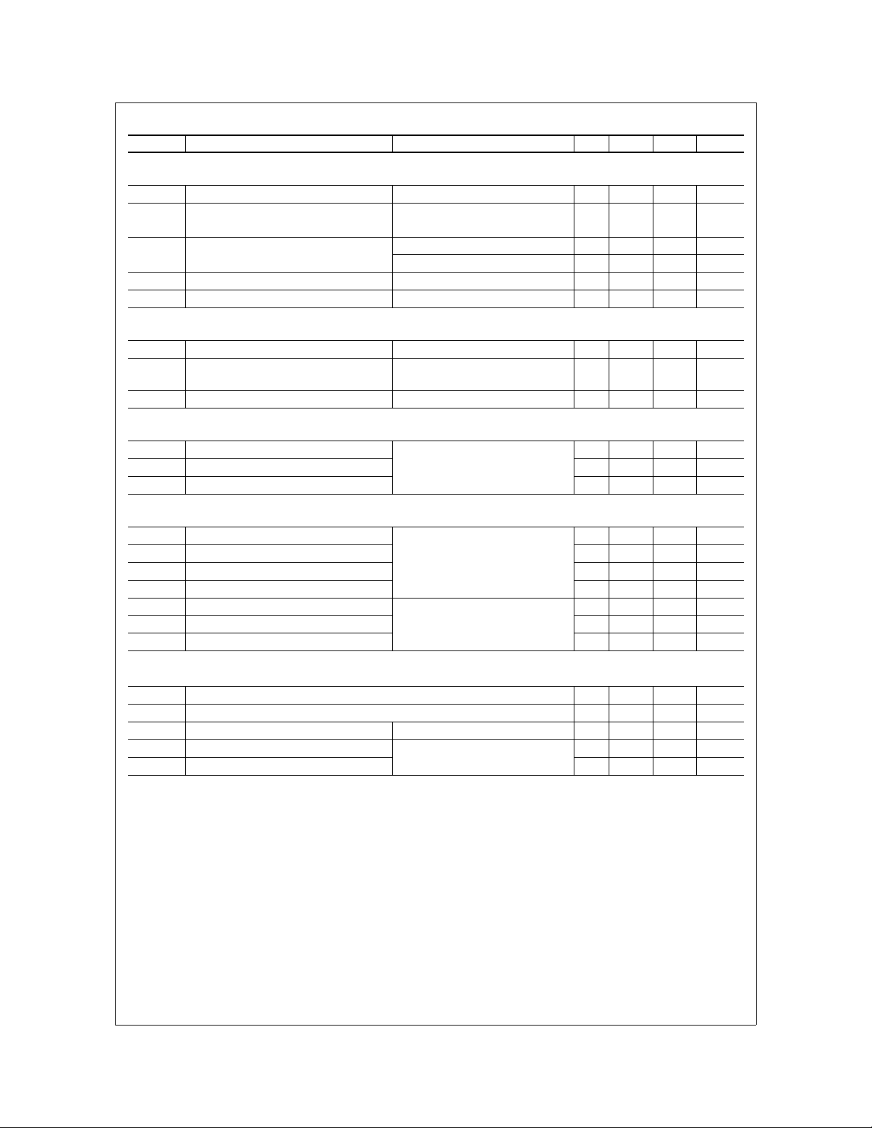
Figure 2. Transfer CharacteristicsFigure 1. On-Region Characteristics
1
10
0
10
℃
, Rev erse Dr ain Cur rent [A]
DR
I
-1
10
0.2 0.4 0.6 0.8 1.0 1.2 1.4
150
℃
25
※
Notes :
1. V
= 0V
GS
2. 250μs Pulse Test
VSD, Sourc e-Drai n voltage [ V]
Figure 3. On-Resistance Variation vs
Drain Current and Gate Voltage
Figure 4. Body Diode Forward Voltage
Variation with Source Current
and Temperature
VDS = 160V
VDS = 400V
VDS = 640V
※
Note : I
2500
2000
1500
1000
Capacitance [pF]
500
0
-1
10
C
= Cgs + Cgd (Cds = shorted)
iss
C
= Cds + C
oss
gd
C
= C
rss
C
iss
C
oss
C
rss
0
10
gd
10
※
1. V
2. f = 1 MHz
1
Notes :
= 0 V
GS
VDS, Drain-Source Voltage [V]
12
10
8
6
4
, Gate-Source Voltage [V]
GS
2
V
0
010203040
QG, Total Gate Charge [nC]
Figure 5. Capacitance Characteristics Figure 6. Gate Charge Characteristics
= 8A
D
www.fairchildsemi.com FQP8N80C/FQPF8N80C/FQPF8N80CYDTU Rev.A 3
Page 4
Typical Characteristics
(Continued)
FQP8N80C/FQPF8N80C/FQPF8N80CYDTU 800V N-Channel MOSFET
1.2
1.1
1.0
, (Normalized)
DSS
BV
0.9
Drain-Source Breakdown Voltage
0.8
-100 -50 0 50 100 150 200
T
, Juncti on Temperature [oC]
J
※
1. V
2. I
Notes :
D
= 0 V
GS
= 250 μA
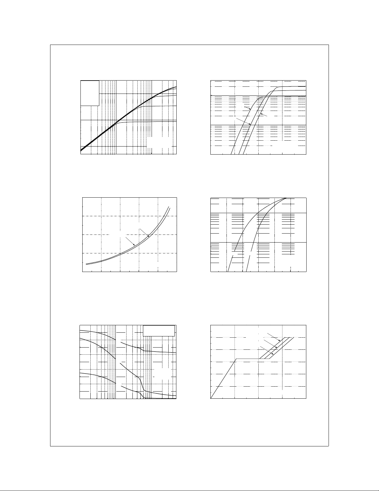
Figure 7. Breakdown Voltage Variation
vs Temperature
2
10
1
10
0
10
, Drai n Current [A]
D
I
-1
10
-2
10
0
10
Operation in This Area
is Limited by R
DS(on)
DC
※
Notes :
1. T
= 25 oC
C
2. T
= 150 oC
J
3. Single Pulse
1
10
2
10
VDS, Drai n-Source Voltage [V]
100 µs
1 ms
10 ms
10 µs
3.0
2.5
2.0
1.5
, ( Normali zed)
1.0
DS(ON)
R
Drain- Source On-Resistance
0.5
0.0
-100 -50 0 50 100 150 200
※
Notes :
= 10 V
1. V
GS
2. I
= 4.0 A
D
TJ, Juncti on Temperature [oC]
Figure 8. On-Resistance Variation
vs Temperature
2
10
1
10
3
10
0
10
, Drai n Current [A]
D
I
-1
10
-2
10
0
10
Operation in This Area
is Limited by R
DS(on)
10 ms
DC
※
Notes :
1. T
= 25 oC
C
2. TJ = 150 oC
3. Single Pulse
1
10
2
10
VDS, Drai n-Source Vol tage [V]
1 ms
100 µs
10 µs
3
10
Figure 9-1. Maximum Safe Operating Area
for FQP8N80C
10
8
6
4
, Drai n Current [A]
D
I
2
0
25 50 75 100 125 150
TC, Case Temperature [℃]
Figure 10. Maximum Drain Current
vs Case Temperature
FQP8N80C/FQPF8N80C/FQPF8N80CYDTU Rev.A 4
Figure 9-2. Maximum Safe Operating Area
for FQPF8N80C
www.fairchildsemi.com
Page 5

Typical Characteristics
(Continued)
FQP8N80C/FQPF8N80C/FQPF8N80CYDTU 800V N-Channel MOSFET
0
10
D=0.5
0.2
-1
10
0.1
0.05
0.02
(t), Thermal Response
JC
0.01
θ
Z
-2
10
-5
10
single pulse
-4
10
-3
10
t
, Square Wave Pulse Duration [sec]
1
-2
10
※
Notes :
(t) = 0.7 ℃/W Ma x.
1. Z
θ
JC
2. D uty F acto r, D =t
3. TJM - TC = PDM * Z
-1
10
10
1/t2
(t)
θ
JC
0
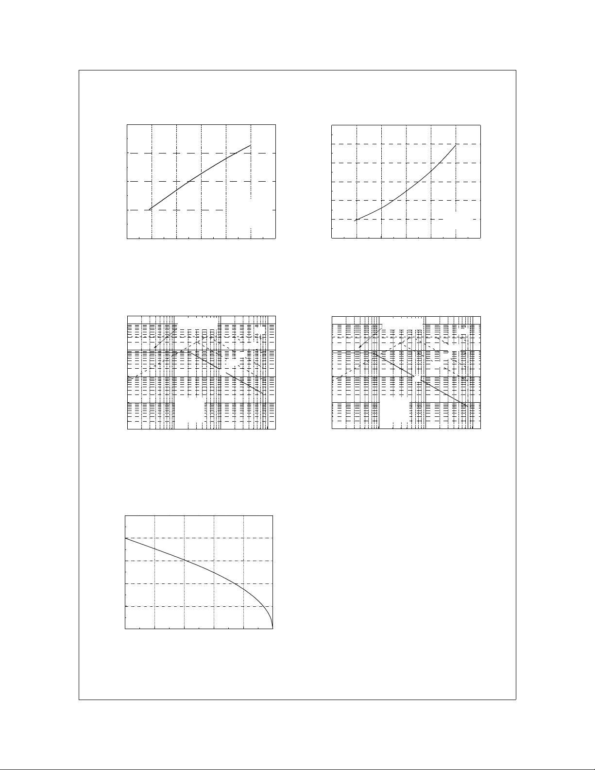
Figure 11-1. Transient Thermal Response Curve for FQP8N80C
0
D=0.5
10
※
0.2
0.1
0.05
-1
10
0.02
0.01
(t), Th e rm a l R e sp on s e
JC
θ
Z
-2
10
-5
10
sin g le pu lse
-4
10
-3
10
-2
10
t1, Square Wave Pulse Duration [sec]
Notes :
1. Z
(t) = 2.1 ℃/W Ma x.
θ
JC
2. D uty F actor, D =t
3. TJM - TC = PDM * Z
-1
10
1/t2
θ
JC
0
10
1
10
(t)
1
10
Figure 11-2. Transient Thermal Response Curve for FQPF8N80C
FQP8N80C/FQPF8N80C/FQPF8N80CYDTU Rev.A 5
www.fairchildsemi.com
Page 6

Gate Charge Test Circuit & Waveform
Resistive Switching Test Circuit & Waveforms
FQP8N80C/FQPF8N80C/FQPF8N80CYDTU 800V N-Channel MOSFET
FQP8N80C/FQPF8N80C/FQPF8N80CYDTU Rev. A
Unclamped Inductive Switching Test Circuit & Waveforms
5
www.fairchildsemi.com
Page 7

Peak Diode Recovery dv/dt Test Circuit & Waveforms
+
+
V
V
DS
DS
_
_
L
LL
Sam e T ype
Sam e T ype
as DU T
as DU T
• dv/dt controlled by R
• dv/dt controlled by R
•ISDcontrolled by pulse period
•ISDcontrolled by pulse period
G
G
V
V
GS
GS
R
R
Driver
Driver
G
G
DUT
DUT
I
I
SD
SD
V
V
DD
DD
FQP8N80C/FQPF8N80C/FQPF8N80CYDTU 800V N-Channel MOSFET
V
V
GS
GS
( D riv e r )
( D riv e r )
I
I
SD
SD
( D U T )
( D U T )
V
V
DS
DS
( DUT )
( DUT )
G ate Pulse W idth
G ate Pulse W idth
G ate Pulse W idth
--------------------------
--------------------------
--------------------------
D =
D =
D =
Gate Pulse Period
Gate Pulse Period
Gate Pulse Period
IFM, B ody Diode Forw ard C urrent
IFM, B ody D iode Forw ard C urrent
I
I
RM
RM
Body D iode R everse Current
Body D iode R everse Current
Body D iode R ecovery dv/dt
Body D iode R ecovery dv/dt
V
V
SD
SD
Body D iode
Body D iode
Forw ard Volta
Forw ard Volta
g e D rop
g e D rop
di/dt
di/dt
10V
10V
V
V
DD
DD
FQP8N80C/FQPF8N80C/FQPF8N80CYDTU Rev. A
6
www.fairchildsemi.com
Page 8

Peak Diode Recovery dv/dt Test Circuit & Waveforms
+
+
V
V
DS
DS
_
_
L
LL
Sam e T ype
Sam e T ype
as DU T
as DU T
• dv/dt controlled by R
• dv/dt controlled by R
•ISDcontrolled by pulse period
•ISDcontrolled by pulse period
G
G
V
V
GS
GS
R
R
Driver
Driver
G
G
DUT
DUT
I
I
SD
SD
V
V
DD
DD
FDB037N06 N-Channel PowerTrench
®
MOSFET
V
V
GS
GS
( D riv e r )
( D riv e r )
I
I
SD
SD
( D U T )
( D U T )
V
V
DS
DS
( DUT )
( DUT )
G ate Pulse W idth
G ate Pulse W idth
G ate Pulse W idth
--------------------------
--------------------------
--------------------------
D =
D =
D =
Gate Pulse Period
Gate Pulse Period
Gate Pulse Period
IFM, B ody D iode Forw ard C urrent
IFM, B ody D iode Forw ard C urrent
I
I
RM
RM
Body D iode R everse Current
Body D iode R everse Current
Body D iode R ecovery dv/dt
Body D iode R ecovery dv/dt
V
V
SD
SD
Body D iode
Body D iode
Forw ard Volta
Forw ard Volta
g e D rop
g e D rop
di/dt
di/dt
10V
10V
V
V
DD
DD
FQP8N80C/FQPF8N80C/FQPF8N80CYDTU Rev. A
7
www.fairchildsemi.com
Page 9

Package Dimensions
FQP8N80C/FQPF8N80CFQPF8N80CYDTU 800V N-Channel MOSFET
TO-220
(1.70)
9.20 ±0.2013.08 ±0.20
1.30 ±0.10
(1.46)
(1.00)
1.27 ±0.10
9.90 ±0.20
(8.70)
ø3.60 ±0.10
(3.70)(3.00)
(45°)
1.52 ±0.10
2.80 ±0.1015.90 ±0.20
18.95MAX.
4.50 ±0.20
+0.10
1.30
–0.05
0.80 ±0.10
2.54TYP
±0.20]
[2.54
2.54TYP
±0.20]
[2.54
10.00 ±0.20
FQP8N80C/FQPF8N80C/FQPF8N80CYDTU Rev.A 8
10.08 ±0.30
0.50
+0.10
–0.05
2.40 ±0.20
Dimensions in Millimeters
www.fairchildsemi.com
Page 10

FQP8N80C/FQPF8N80C/FQPF8N80CYDTU 800V N-Channel MOSFET
Package Dimensions
3.30 ±0.10
15.80 ±0.20
(Continued)
10.16 ±0.20
(7.00)
TO-220F
ø3.18 ±0.10
6.68 ±0.20
(1.00x45°)
2.54
(0.70)
±0.20
15.87 ±0.20
9.75 ±0.30
MAX1.47
0.80 ±0.10
0.35 ±0.10
2.54TYP
[2.54
±0.20]
#1
9.40 ±0.20
(30°)
2.54TYP
[2.54
±0.20]
4.70 ±0.20
0.50
+0.10
–0.05
2.76 ±0.20
FQP8N80C/FQPF8N80C/FQPF8N80CYDTU Rev.A
Dimensions in Millimeters
9
www.fairchildsemi.com
Page 11

FQF8N80C/FQPF8N80C/FQPF8N80CYDTU 800V N-Channel MOSFET
FQP8N80C/FQPF8N80C/FQPF8N80CYDTU Rev.A
10
www.fairchildsemi.com
Page 12

TRADEMARKS
The following includes registered and unregistered trademarks and service marks, owned by Fairchild Semiconductor and/or its global subsidiaries, and is not
intended to be an exhaustive list of all such trademarks.
Build it Now™
CorePLUS™
CorePOWER™
CROSSVOLT™
CTL™
Current Transfer Logic™
EcoSPARK
EfficentMax™
EZSWITCH™ *
™
Fairchild
Fairchild Semiconductor
FACT Quiet Series™
FACT
FAST
FastvCore™
FlashWriter
FPS™
®
®
tm
®
®
®
®
*
®
F-PFS™
* EZSWITCH™ and FlashWriter
®
are trademarks of System General Corporation, used under license by Fairchild Semiconductor.
®
FRFET
Global Power Resource
Green FPS™
Green FPS™ e-Series™
GTO™
IntelliMAX™
ISOPLANAR™
MegaBuck™
MICROCOUPLER™
MicroFET™
MicroPak™
MillerDrive™
MotionMax™
Motion-SPM™
OPTOLOGIC
OPTOPLANAR
PDP SPM™
Power-SPM™
PowerTrench
PowerXS™
®
®
®
tm
®
SM
Programmable Active Droop™
®
QFET
QS™
Quiet Series™
RapidConfigure™
™
Saving our world, 1mW /W /kW at a time™
SmartMax™
SMART START™
®
SPM
STEALTH™
SuperFET™
SuperSOT™-3
SuperSOT™-6
SuperSOT™-8
SupreMOS™
SyncFET™
®
The Power Franchise
®
TinyBoost™
tm
TinyBuck™
®
TinyLogic
TINYOPTO™
TinyPower™
TinyPWM™
TinyWire™
μSerDes™
®
UHC
Ultra FRFET™
UniFET™
VCX™
VisualMax™
XS™
DISCLAIMER
FAIRCHILD SEMICONDUCTOR RESERVES THE RIGHT TO MAKE CHANGES WITHOUT FURTHER NOTICE TO ANY PRODUCTS HEREIN TO IMPROVE
RELIABILITY, FUNCTION, OR DESIGN. FAIRCHILD DOES NOT ASSUME ANY LIABILITY ARISING OUT OF THE APPLICATION OR USE OF ANY
PRODUCT OR CIRCUIT DESCRIBED HEREIN; NEITHER DOES IT CONVEY ANY LICENSE UNDER ITS PATENT RIGHTS, NOR THE RIGHTS OF OTHERS.
THESE SPECIFICATIONS DO NOT EXPAND THE TERMS OF FAIRCHILD’S WORLDWIDE TERMS AND CONDITIONS, SPECIFICALLY THE WARRANTY
THEREIN, WHICH COVERS THESE PRODUCTS.
FQP8N80C/FQPF8N80C/FQPF8N80CYDTU 800V N-Channel MOSFET
LIFE SUPPORT POLICY
FAIRCHILD’S PRODUCTS ARE NOT AUTHORIZED FOR USE AS CRITICAL COMPONENTS IN LIFE SUPPORT DEVICES OR SYSTEMS WITHOUT THE
EXPRESS WRITTEN APPROVAL OF FAIRCHILD SEMICONDUCTOR CORPORATION.
As used herein:
1. Life support devices or systems are devices or systems which, (a) are
intended for surgical implant into the body or (b) sup port or sust ain life ,
and (c) whose failure to perform when properly used in accord ance with
instructions for use provided in the labeling, can be reasonably
expected to result in a significant injury of the user.
ANTI-COUNTERFEITING POLICY
Fairchild Semiconductor Corporation’s Anti-Counterfeiting Policy. Farichild’s Anti-Counterfeiting Policy is also stated on our external website,
www.fairchildsemi.com, under Sales Support
.
2. A critical component in any component of a life support, device, or
system whose failure to perform can be reasonably expected to cause
the failure of the life support device or system, or to affect its safety or
effectiveness.
Counterfeiting of semiconductor parts is a growing problem in the industry. All manufactures of semiconductor products are experi encing counterfeiting of the ir
parts. Customers who inadvertently purchase counterfeit parts experie nce many pr oble ms such as loss o f brand reputat ion , substa ndard p erf ormance , faile d
application, and increased cost of production and manufacturing delays. Fairchild is taking strong measures to protect ourselves and our customers from the
proliferation of counterfeit parts. Farichild strongly encourages custo mers to purchase Farichild p arts either di rectly from Fairchild or from Authorized Fairchil d
Distributors who are listed by country on our web page cited above. Products customers buy either from fairchild directly or from Authorized Fairchild
Distributors are genuine parts, have full traceability, meet Fairchild’s quality standards for handing and storage and provide access to Farichild’s full range of
up-to-date technical and product information. Fairchild and our Authorized Distributors will stand behind all warranties and will appropriately address and
warranty issues that may arise. Fairchild will not provide any warranty coverage or other assistance for parts bought from Unauthorized Sources. Farichild is
committed to combat this global problem and encourage our customers to do their part in stopping this practi ce by buying direct or from a uthorized distributors.
PRODUCT STATUS DEFINITIONS
Definition of Terms
Datasheet Identification Product Status Definition
Advance Information Formative / In Design
Preliminary First Production
No Identification Needed Full Production
Obsolete Not In Production
FQP8N80C/FQPF8N80C/FQPF8N80CYDTU Rev. A
Datasheet contains the design specifications for product development. Specifications
may change in any manner without notice.
Datasheet contains preliminary data; supplementary data will be published at a later
date. Fairchild Semiconductor reserves the right to make changes at any time without
notice to improve design.
Datasheet contains final specifications. Fairchild Semiconductor reserves the right to
make changes at any time without notice to improve the design.
Datasheet contains specifications on a product that is discontinued by Fairchild
Semiconductor. The datasheet is for reference information only.
Rev. I37
1
www.fairchildsemi.com1
 Loading...