

Fairchild FQP10N60C, FQPF10N60C service manual
现货库存、技术资料、百科信息、热点资讯,精彩尽在鼎好!
FQP10N60C / FQPF10N60C
600V N-Channel MOSFET
FQP10N60C / FQPF10N60C 600V N-Channel MOSFET
April 2007
®
QFET
Features
• 9.5A, 600V, R
• Low gate charge ( typical 44 nC)
• Low Crss ( typical 18 pF)
•Fast switching
• 100% avalanche tested
• Improved dv/dt capability
= 0.73Ω @VGS = 10 V
DS(on)
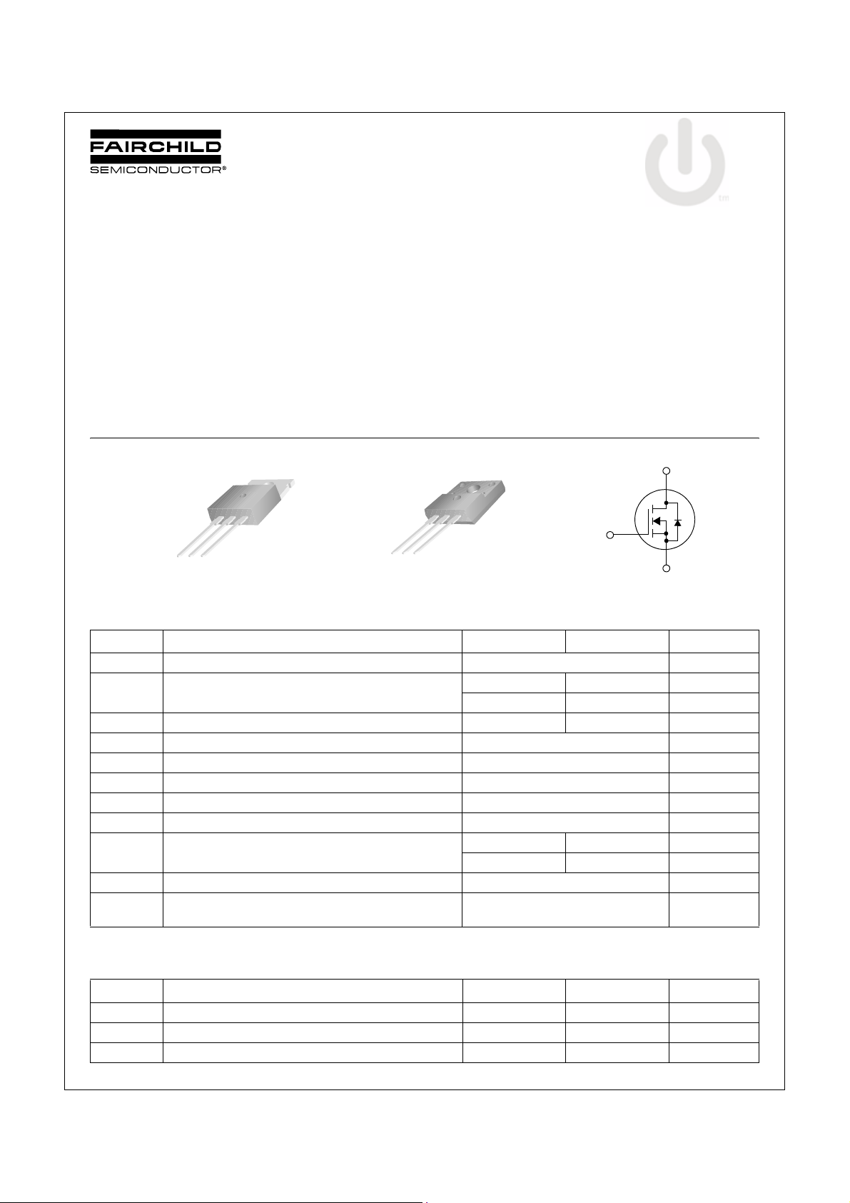
GSD
TO-220
FQP Series
GSD
Description
These N-Channel enhancement mode power field effect transistors are produced using Fairchild’s proprietary, planar stripe,
DMOS technology.
This advanced technology has been especially tailored to minimize on-state resistance, provide superior switching performance, and withstand high energy pulse in the avalanche and
commutation mode. These devices are well suited for high efficiency switched mode power supplies, active power factor correction, electronic lamp ballasts based on half bridge topology.
D
G
TO-220F
FQPF Series
S
Absolute Maximum Ratings
Symbol Parameter FQP10N60C FQPF10N60C Units
V
DSS
I
D
I
DM
V
GSS
E
AS
I
AR
E
AR
dv/dt Peak Diode Recovery dv/dt
P
D
T
, T
J
STG
T
L
* Drain current limited by maximum junction temperature.
Drain-Source Voltage 600 V
Drain Current - Continuous (TC = 25°C) 9.5 9.5 * A
- Continuous (T
Drain Current - Pulsed
Gate-Source Voltage ± 30 V
Single Pulsed Avalanche Energy
Avalanche Current
Repetitive Avalanche Energy
Power Dissipation (TC = 25°C) 156 50 W
- Derate above 25°C 1.25 0.4 W/°C
Operating and Storage Temperature Range -55 to +150 °C
Maximum lead temperature for soldering purposes,
1/8" from case for 5 seconds
= 100°C) 5.7 5.7 * A
C
(Note 1)
(Note 2)
(Note 1)
(Note 1)
(Note 3)
38 38 * A
700 mJ
9.5 A
15.6 mJ
4.5 V/ns
300 °C
Thermal Characteristics
Symbol Parameter FQP10N60C FQPF10N60C Units
R
θJC
R
θCS
R
θJA
©2007 Fairchild Semiconductor Corporation 1 www.fairchildsemi.com
FQP10N60C / FQPF10N60C Rev. C
Thermal Resistance, Junction-to-Case 0.8 2.5 °C/W
Thermal Resistance, Case-to-Sink Typ. 0.5 -- °C/W
Thermal Resistance, Junction-to-Ambient 62.5 62.5 °C/W
Package Marking and Ordering Information
Device Marking Device Package Reel Size Tape Width Quantity
FQP10N60C FQP10N60C TO-220 -- -- 50
FQPF10N60C FQPF10N60C TO-220F -- -- 50
FQP10N60C / FQPF10N60C 600V N-Channel MOSFET
Electrical Characteristics T
= 25°C unless otherwise noted
C
Symbol Parameter Test Conditions Min Typ Max Units
Off Characteristics
BV
DSS
∆BV
DSS
∆T
J
I
DSS
I
GSSF
I
GSSR
On Characteristics
V
GS(th)
R
DS(on)
g
FS
Dynamic Characteristics
C
iss
C
oss
C
rss
Drain-Source Breakdown Voltage VGS = 0 V, ID = 250 µA 600 -- -- V
/
Breakdown Voltage Temperature
ID = 250 µA, Referenced to 25°C -- 0.7 -- V/°C
Coefficient
Zero Gate Voltage Drain Current VDS = 600 V, VGS = 0 V -- -- 1 µA
= 480 V, TC = 125°C -- -- 10 µA
V
DS
Gate-Body Leakage Current, Forward VGS = 30 V, VDS = 0 V -- -- 100 nA
Gate-Body Leakage Current, Reverse VGS = -30 V, VDS = 0 V -- -- -100 nA
Gate Threshold Voltage VDS = VGS, ID = 250 µA2.0--4.0V
Static Drain-Source
VGS = 10 V, ID = 4.75 A -- 0.6 0.73 Ω
On-Resistance
Forward Transconductance VDS = 40 V , ID = 4.75 A (Note 4) -- 8.0 -- S
Input Capacitance VDS = 25 V, VGS = 0 V,
Output Capacitance -- 166 215 pF
f = 1.0 MHz
-- 1570 2040 pF
Reverse Transfer Capacitance -- 18 24 pF
Switching Characteristics
t
d(on)
t
r
t
d(off)
t
f
Q
Q
Q
g
gs
gd
Turn-On Delay Time VDD = 300 V, ID = 9.5A,
R
Turn-On Rise Time -- 69 150 ns
G
Turn-Off Delay Time -- 144 300 ns
Turn-Off Fall Time -- 77 165 ns
Total Gate Charge VDS = 480 V, ID = 9.5A,
V
Gate-Source Charge -- 6.7 -- nC
GS
Gate-Drain Charge -- 18.5 -- nC
Drain-Source Diode Characteristics and Maximum Ratings
I
S
I
SM
V
SD
t
rr
Q
rr
Notes:
1. Repetitive Rating : Pulse width limited by maximum junction temperature
2. L = 14.2mH, IAS = 9.5 A, VDD = 50V, RG = 25 Ω, Starting TJ = 25°C
≤ 9.5A, di/dt ≤ 200A/µs, VDD ≤ BV
3. I
SD
4. Pulse Test : Pulse width ≤ 300µs, Duty cycle ≤ 2%
5. Essentially independent of operating temp er at ur e
Maximum Continuous Drain-Source Diode Forward Current -- -- 9.5 A
Maximum Pulsed Drain-Source Diode Forward Current -- -- 38 A
Drain-Source Diode Forward Voltage VGS = 0 V, IS = 9.5 A -- -- 1.4 V
Reverse Recovery Time VGS = 0 V, IS = 9.5 A,
dI
Reverse Recovery Charge -- 4.2 -- µC
Starting TJ = 25°C
DSS,
F
-- 23 55 ns
= 25 Ω
(Note 4, 5)
-- 44 57 nC
= 10 V
(Note 4, 5)
-- 420 -- ns
/ dt = 100 A/µs (Note 4)
FQP10N60C / FQPF10N60C Rev. C
2 www.fairchildsemi.com
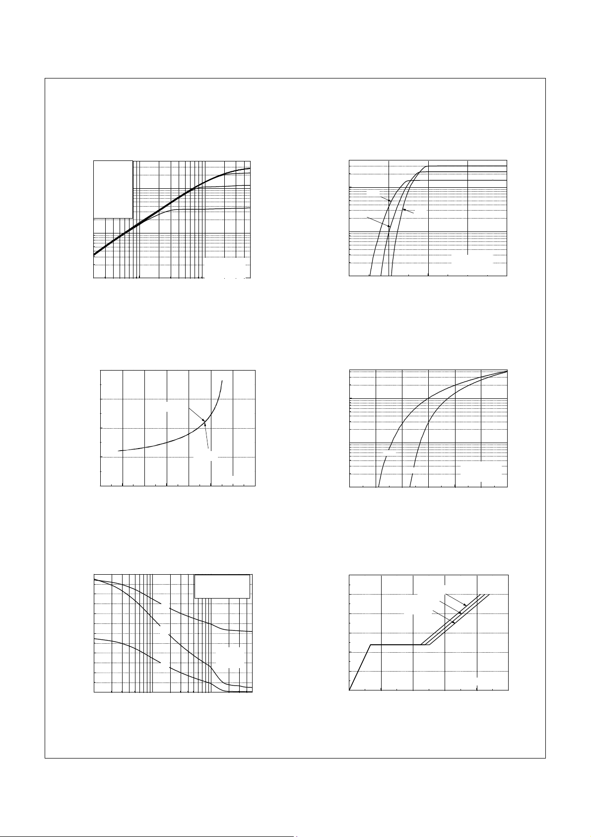
Typical Performance Characteristics
Figure 1. On-Region Characteristics Figure 2. Transfer Characteristics
FQP10N60C / FQPF10N60C 600V N-Channel MOSFET
-55°C
* Notes :
1. V
= 40V
DS
µs Pulse Test
2. 250
10
10
, Drain Current [A]
D
I
10
V
Top : 15.0 V
10.0 V
8.0 V
1
7.0 V
6.5 V
6.0 V
5.5 V
5.0 V
Bottom : 4.5 V
0
-1
GS
0
10
VDS, Drain-Source Voltage [V]
1
10
150°C
25°C
0
10
, Drain Current [A]
D
I
-1
10
246810
VGS, Gate-Source Voltage [V]
10
* Notes :
1. 250
2. T
1
µs Pulse Test
= 25°C
C
Figure 3. On-Resistance Variation vs. Figure 4. Body Diode Forward Voltage
Drain Current and Gate Voltage Variation vs. Source Current
and Temperatue
25°C
* Notes :
1. V
2. 250
2.0
1.5
[Ω],
1.0
DS(ON)
R
0.5
VGS = 10V
VGS = 20V
Drain-Source On-Resistance
0.0
0 5 10 15 20 25 30 35
ID, Drain Current [A]
* Note : TJ = 25°C
1
10
0
10
150°C
, Reverse Drain Current [A]
DR
I
-1
10
0.2 0.4 0.6 0.8 1.0 1.2 1.4
VSD, Source-Drain voltage [V]
= 0V
GS
µs Pulse Te st
Figure 5. Capacitance Characteristics Figure 6. Gate Charge Characteristics
3000
2500
C
2000
1500
1000
Capacitance [pF]
500
0
-1
10
iss
C
oss
C
rss
0
10
VDS, Drain-Source Voltage [V]
FQP10N60C / FQPF10N60C Rev. C
C
= Cgs + Cgd (Cds = shorted)
iss
C
= Cds + C
oss
gd
C
= C
rss
gd
* Notes ;
1. V
2. f = 1 MHz
1
10
12
10
8
= 0 V
GS
6
4
, Gate-Source Voltage [V]
2
GS
V
0
0 1020304050
QG, Total Gate Cha rg e [nC]
3 www.fairchildsemi.com
VDS = 120V
VDS = 300V
VDS = 480V
* Note : ID = 9.5A
 Loading...