

Fairchild FQD6N40C, FQU6N40C service manual
FQD6N40C / FQU6N40C
FQD6N40C / FQU6N40C
400V N-Channel MOSFET
General Description
These N-Channel enhancement mode power field effect
transistors are produced using Fairchild’s proprietary,
planar stripe, DMOS technology.
This advanced technology has been especially tailored to
minimize on-state resistance, provide superior switching
performance, and withstand high energy pulse in the
avalanche and commutation mode. These devices are well
suited for high efficiency switched mode power supplies,
electronic lamp ballasts based on half bridge topology.
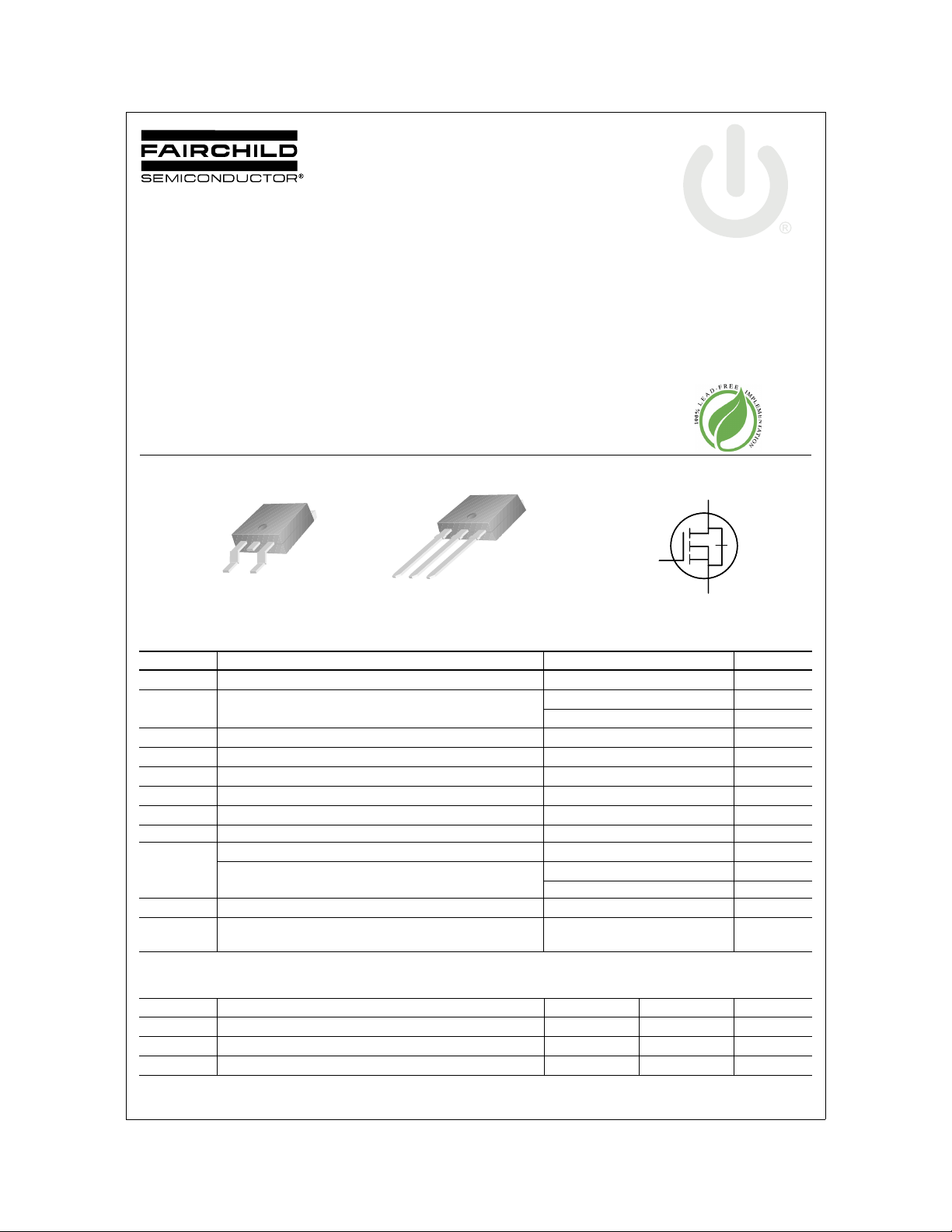
D
GS
D-PAK
FQD Series
GSD
Features
• 4.5A, 400V, R
• Low gate charge ( typical 16nC)
• Low Crss ( typical 15pF)
• Fast switching
• 100% avalanche tested
• Improved dv/dt capability
• RoHS Compliant
I-PAK
FQU Series
= 1.0 Ω @VGS = 10 V
DS(on)
!!!!
!!!!
G
October 2008
QFET
D
!!!!
!!!!
!!!!
!!!!
####
####
""""
""""
!!!!
!!!!
!!!!
!!!!
!!!!
!!!!
S
®
Absolute Maximum Ratings T
= 25°C unless otherwise noted
C
Symbol Parameter FQD6N40C / FQU6N40C Units
V
DSS
I
D
I
DM
V
GSS
E
AS
I
AR
E
AR
dv/dt Peak Diode Recovery dv/dt
P
D
Drain-Source Voltage 400 V
Drain Current
- Continuous (T
- Continuous (T
Drain Current - Pulsed
= 25°C)
C
= 100°C)
C
(Note 1)
4.5 A
2.7 A
18 A
Gate-Source Voltage ± 30 V
Single Pulsed Avalanche Energy
Avalanche Current
Repetitive Avalanche Energy
Power Dissipation (TA = 25°C)*
Power Dissipation (T
= 25°C)
C
(Note 2)
(Note 1)
(Note 1)
(Note 3)
270 mJ
4.5 A
4.8 mJ
4.5 V/ns
2.5 W
48 W
- Derate above 25°C 0.38 W/°C
, T
T
J
STG
T
L
Operating and Storage Temperature Range -55 to +150 °C
Maximum lead temperature for soldering purposes,
1/8" from case for 5 seconds
300 °C
Thermal Characteristics
Symbol Parameter Typ Max Units
R
θJC
R
θJA
R
θJA
* When mounted on the minimum pad size recommended (PCB Mount)
Thermal Resistance, Junction-to-Case -- 2.6 °C/W
Thermal Resistance, Junction-to-Ambient.* -- 50 °C/W
Thermal Resistance, Junction-to-Ambient. -- 110 °C/W
©2008 Fairchild Semiconductor Internationa Rev. A1, October 2008
FQD6N40C / FQU6N40C
Electrical Characteristics T
= 25°C unless otherwise noted
C
Symbol Parameter Test Conditions Min Typ Max Units
Off Characteristics
BV
DSS
∆BV
DSS
/ ∆T
I
DSS
I
GSSF
I
GSSR
Drain-Source Breakdown Voltage
Breakdown Voltage Temperature
Coefficient
J
Zero Gate Voltage Drain Current
Gate-Body Leakage Current, Forward
Gate-Body Leakage Current, Reverse
V
= 0 V, ID = 250 µA
GS
= 250 µA, Referenced to 25°C
I
D
V
= 400 V, VGS = 0 V
DS
= 320 V, TC = 125°C
V
DS
V
= 30 V, VDS = 0 V
GS
V
= -30 V, VDS = 0 V
GS
400 -- -- V
-- 0.54 -- V/°C
-- -- 1 µA
-- -- 10 µA
-- -- 100 nA
-- -- -100 nA
On Characteristics
V
R
g
FS
GS(th)
DS(on)
Gate Threshold Voltage
Static Drain-Source
On-Resistance
Forward Transconductance
V
= VGS, ID = 250 µA
DS
= 10 V, ID = 2.25A
V
GS
V
= 40 V, ID = 2.25A
DS
(Note 4)
2.0 -- 4.0 V
-- 0.83 1 Ω
-- 4.7 -- S
Dynamic Characteristics
C
iss
C
oss
C
rss
Input Capacitance
Output Capacitance -- 80 105 pF
Reverse Transfer Capacitance -- 15 20 pF
V
= 25 V, VGS = 0 V,
DS
f = 1.0 MHz
-- 480 625 pF
Switching Characteristics
t
d(on)
t
r
t
d(off)
t
f
Q
Q
Q
g
gs
gd
Turn-On Delay Time
Turn-On Rise Time -- 65 140 ns
Turn-Off Delay Time -- 21 55 ns
Turn-Off Fall Time -- 38 85 ns
Total Gate Charge
Gate-Source Charge -- 2.3 -- nC
Gate-Drain Charge -- 8.2 -- nC
V
= 200 V, ID = 6A,
DD
R
= 25 Ω
G
(Note 4, 5)
V
= 320 V, ID = 6A,
DS
V
GS
(Note 4, 5)
= 10 V
-- 13 35 ns
-- 16 20 nC
Drain-Source Diode Characteristics and Maximum Ratings
I
S
I
SM
V
SD
t
rr
Q
rr
Notes:
1. Repetitive Rating : Pulse width limited by maximum junction temperature
2. L = 13.7 mH, IAS = 6 A, VDD = 50V, RG = 25 Ω, Starting TJ = 25°C
3. ISD ≤ 6A, di/dt ≤ 200A/µs, VDD ≤ BV
4. Pulse Test : Pulse width ≤ 300µs, Duty cycle ≤ 2%
5. Essentially independent of operating temperature
©2008 Fairchild Semiconductor Internationa Rev. A1, October 2008
Maximum Continuous Drain-Source Diode Forward Current -- -- 4.5 A
Maximum Pulsed Drain-Source Diode Forward Current -- -- 18 A
V
Drain-Source Diode Forward Voltage
Reverse Recovery Time
Reverse Recovery Charge -- 1.7 -- µC
Starting TJ = 25°C
DSS,
= 0 V, IS = 4.5 A
GS
= 0 V, IS = 6 A,
V
GS
dI
/ dt = 100 A/µs
F
-- -- 1.4 V
-- 230 -- ns
(Note 4)
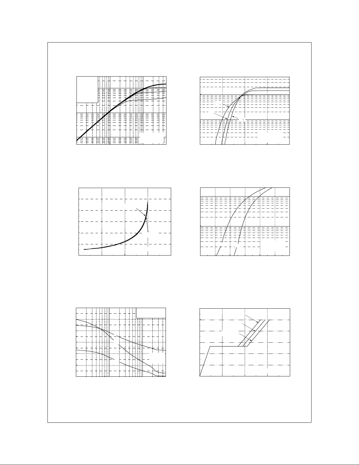
Typical Characteristics
FQD6N40C / FQU6N40C
1
10
0
10
, Dra in C u rr en t [A ]
D
I
-1
10
10
V
Top : 1 5 .0 V
10.0 V
8.0 V
7.0 V
6.5 V
6.0 V
5.5 V
Bottom : 5.0 V
-1
GS
0
10
VDS, Drain-Source Voltage [V]
1
10
150oC
%
Note s :
1. 250&s Pulse Test
$
= 25
2. T
C
1
10
25oC
0
10
, Drain Current [A]
D
I
-1
10
246810
VGS, Gate-Source Voltage [V]
-55oC
Figure 1. On-Region Characteristics Figure 2. Transfer Characteristics
3.5
3.0
2.5
],
'
[
2.0
DS(ON)
R
1.5
Drain-Source On-Resistance
1.0
0.5
0 5 10 15 20
VGS = 10V
VGS = 20V
%
ID, Drain Current [A]
Note : T
1
10
$
= 25
J
0
10
, Reverse Drain Current [A]
DR
I
-1
10
0.2 0.4 0.6 0.8 1.0 1.2 1.4
$
150
VSD, Source-Drain voltage [V]
$
25
%
Notes :
= 40V
1. V
DS
2. 25 0&s Pulse Test
%
Note s :
= 0V
1. V
GS
2. 250&s Pulse T es t
Figure 3. On-Resistance Variation vs
Drain Current and Gate Voltage
Figure 4. Body Diode Forward Voltage
Variation with Source Current
and Temperature
1200
1000
800
600
400
Capacitance [pF]
200
0
-1
10
C
= C
+ Cgd (Cds = shorted )
iss
gs
C
= Cds + C
oss
gd
C
= C
rss
gd
C
iss
C
oss
%
Notes ;
C
rss
0
10
1. V
2. f = 1 MH z
1
10
= 0 V
GS
12
10
8
6
4
, Gate-Source Voltage [V]
GS
2
V
0
0 5 10 15 20
VDS = 320V
VDS, Drain-Source Voltage [V]
VDS = 80V
VDS = 200V
QG, Tota l G a te C h a rg e [n C ]
%
Note : I
= 6A
D
Figure 5. Capacitance Characteristics Figure 6. Gate Charge Characteristics
©2008 Fairchild Semiconductor Internationa Rev. A1, October 2008
 Loading...