

FQD17P06 / FQU17P06
©2009 Fairchild S emiconductor Corporation Rev. A3.January 2009
FQD17P06 / FQU17P06
60V P-Channel MOSFET
General Description
These P-Channel enhancement mode power field effect
transistors are produced using Fairchild’s proprietary,
planar stripe, DMOS technology.
This advanced technology has been especially tailored to
minimize on-state resistance, provide superior switching
performance, and withstand a high energy pulse in the
avalanche and commutation modes. These devices are
well suited for low voltage applications such as automotive,
DC/DC converters, and high efficiency switching for power
management in portable and battery operated products.
Features
• -12A, -60V, R
DS(on)
= 0.135Ω @VGS = -10 V
• Low gate charge ( typical 21 nC)
• Low Crss ( typical 80 pF)
• Fast switching
• 100% avalanche tested
• Improved dv/dt capability
Absolute Maximum Ratings T
C
= 25°C unless otherwise noted
Thermal Characteristics
Symbol Parameter FQD17P06 / FQU17P06 Units
V
DSS
Drain-Source Voltage -60 V
I
D
Drain Current
- Continuous (T
C
= 25°C)
-12 A
- Continuous (T
C
= 100°C)
-7.6 A
I
DM
Drain Current - Pulsed
(Note 1)
-48 A
V
GSS
Gate-Source Voltage ± 25 V
E
AS
Single Pulsed Avalanche Energy
(Note 2)
300 mJ
I
AR
Avalanche Current
(Note 1)
-12 A
E
AR
Repetitive Avalanche Energy
(Note 1)
4.4 mJ
dv/dt Peak Diode Recovery dv/dt
(Note 3)
-7.0 V/ns
P
D
Power Dissipation (TA = 25°C) *
2.5 W
Power Dissipation (T
C
= 25°C)
44 W
- Derate above 25°C 0.35 W/°C
T
J
, T
STG
Operating and Storage Temperature Range -55 to +150 °C
T
L
Maximum lead temperature for soldering purposes,
1/8" from case for 5 seconds
300 °C
Symbol Parameter Typ Max Units
R
θJC
Thermal Resistance, Junction-to-Case -- 2.85 °C/W
R
θJA
Thermal Resistance, Junction-to-Ambient * -- 50 °C/W
R
θJA
Thermal Resistance, Junction-to-Ambient -- 110 °C/W
* When mounted on the minimum pad size recommended (PCB Mount)
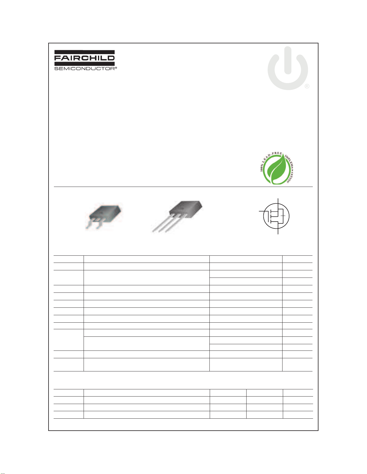
I-PAK
FQU Series
D-PAK
FQD Series
G
S
D
G
S
D
!!!!
!!!!
!!!!
""""
####
!!!!
!!!!
!!!!
!!!!
!!!!
!!!!
""""
####
!!!!
!!!!
!!!!
S
D
G
January 2009
QFET
®
• RoHS Compliant
FQD17P06 / FQU17P06
Rev. A3.January 2009©2009 Fairchild S emiconductor Corporation
Elerical Characteristics T
C
= 25°C unless otherwise noted
Notes:
1. Repetitive Rating : Pulse width limited by maximum junction temperature
2. L = 2.4mH, I
AS
= -12A, VDD = -25V, RG = 25 Ω, Starting TJ = 25°C
3. ISD! -17A, di/dt ! 300A/µs, VDD! BV
DSS,
Starting TJ = 25°C
4. Pulse Test : Pulse width ! 300µs, Duty cycle ! 2%
5. Essentially independent of operating temperature
Symbol Parameter Test Conditions Min Typ Max Units
Off Characteristics
BV
DSS
Drain-Source Breakdown Voltage
V
GS
= 0 V, ID = -250 µA
-60 -- -- V
∆BV
DSS
/ ∆T
J
Breakdown Voltage Temperature
Coefficient
I
D
= -250 µA, Referenced to 25°C
-- -0.06 -- V/°C
I
DSS
Zero Gate Voltage Drain Current
V
DS
= -60 V, VGS = 0 V
-- -- -1 µA
V
DS
= -48 V, TC = 125°C
-- -- -10 µA
I
GSSF
Gate-Body Leakage Current, Forward
V
GS
= -25 V, VDS = 0 V
-- -- -100 nA
I
GSSR
Gate-Body Leakage Current, Reverse
V
GS
= 25 V, VDS = 0 V
-- -- 100 nA
On Characteristics
V
GS(th)
Gate Threshold Voltage
V
DS
= VGS, ID = -250 µA
-2.0 -- -4.0 V
R
DS(on)
Static Drain-Source
On-Resistance
V
GS
= -10 V, ID = -6.0 A
-- 0.11 0.135 Ω
g
FS
Forward Transconductance
V
DS
= -30 V, ID = -6.0 A
-- 8.7 -- S
Dynamic Characteristics
C
iss
Input Capacitance
V
DS
= -25 V, VGS = 0 V,
f = 1.0 MHz
-- 690 900 pF
C
oss
Output Capacitance -- 325 420 pF
C
rss
Reverse Transfer Capacitance -- 80 105 pF
Switching Characteristics
t
d(on)
Turn-On Delay Time
VDD = -30 V, ID = -8.5 A,
R
G
= 25 Ω
-- 13 35 ns
t
r
Turn-On Rise Time -- 100 210 ns
t
d(off)
Turn-Off Delay Time -- 22 55 ns
t
f
Turn-Off Fall Time -- 60 130 ns
Q
g
Total Gate Charge
V
DS
= -48 V, ID = -17 A,
V
GS
= -10 V
-- 21 27 nC
Q
gs
Gate-Source Charge -- 4.2 -- nC
Q
gd
Gate-Drain Charge -- 10 -- nC
Drain-Source Diode Characteristics and Maximum Ratings
I
S
Maximum Continuous Drain-Source Diode Forward Current -- -- -12 A
I
SM
Maximum Pulsed Drain-Source Diode Forward Current -- -- -48 A
V
SD
Drain-Source Diode Forward Voltage
V
GS
= 0 V, IS = -12 A
-- -- -4.0 V
t
rr
Reverse Recovery Time
V
GS
= 0 V, IS = -17 A,
dI
F
/ dt = 100 A/µs
-- 92 -- ns
Q
rr
Reverse Recovery Charge -- 0.32 -- µC
(Note 4)
(Note 4, 5)
(Note 4, 5)
(Note 4)

FQD17P06 / FQU17P06
©2009 Fairchild S emiconductor Corporation Rev. A3. Januaary 2 009
0 10 20 30 40 50 60
0.00
0.04
0.08
0.12
0.16
0.20
0.24
0.28
0.32
0.36
0.40
$
Note : T
J
= 25
%
VGS = - 20V
VGS = - 10V
R
DS(on)
[Ω],
Drain-Source On-Resistance
-ID , Drain Current [A]
10
-1
10
0
10
1
10
0
10
1
V
GS
Top : - 15.0 V
- 10.0 V
- 8.0 V
- 7.0 V
- 6.0 V
- 5.5 V
- 5.0 V
Bottom : - 4.5 V
$
Notes :
1. 250&s Pulse Test
2. T
C
= 25
%
-I
D
, Drain Current [A]
-VDS, Drain-Source Voltage [V]
0 4 8 12 16 20 24
0
2
4
6
8
10
12
VDS = -30V
VDS = -48V
$
Note : I
D
= -17 A
-V
GS
, Gate-Source Voltage [V]
QG, Total Gate Charge [nC]
10
-1
10
0
10
1
0
200
400
600
800
1000
1200
1400
1600
1800
2000
C
iss
= Cgs + Cgd (Cds = shorted)
C
oss
= Cds + C
gd
C
rss
= C
gd
$
Notes :
1. V
GS
= 0 V
2. f = 1 MHz
C
rss
C
oss
C
iss
Capacitance [pF]
VDS, Drain-Source Voltage [V]
0.0 0.2 0.4 0.6 0.8 1.0 1.2 1.4 1.6 1.8 2.0 2.2 2.4
10
-1
10
0
10
1
150
%
$
Notes :
1. VGS = 0V
2. 250&s Pulse Test
25
%
-I
DR
, Reverse Drain Current [A]
-VSD , Source-Drain Voltage [V]
2 4 6 8 10
10
-1
10
0
10
1
150
%
25
%
-55
%
$
Notes :
1. V
DS
= -30V
2. 250&s Pulse Test
-I
D
, Drain Current [A]
-VGS , Gate-Source Voltage [V]
Typical Characteristics
Figure 5. Capacitance Characteristics Figure 6. Gate Charge Characteristics
Figure 3. On-Resistance Variation vs.
Drain Current and Gate Voltage
Figure 4. Body Diode Forward Voltage
Variation vs. Source Current
and Temperature
Figure 2. Transfer CharacteristicsFigure 1. On-Region Characteristics

FQD17P06 / FQU17P06
©2009 Fairchild S emiconductor Corporation Rev. A3. January 2009
1 0
-5
1 0
-4
1 0
-3
1 0
-2
1 0
-1
1 0
0
1 0
1
1 0
-2
1 0
-1
1 0
0
$
N o te s :
1 . Z
'
JC
(t ) = 2. 85 %/W M a x.
2 . D u ty F a c to r, D =t
1/t2
3 . TJM - TC = PDM * Z
'
JC
(t )
s in gl e p u ls e
D = 0. 5
0 .0 2
0 .2
0 .0 5
0 .1
0 .0 1
Z
'
JC
( t), T h e r m a l R e s p o n s e
t1, S q u a r e W a v e P u ls e D u ra t i o n [ s e c ]
25 50 75 100 125 150
0
2
4
6
8
10
12
-I
D
, Drain Current [A]
TC, Case Temperature [%]
10
0
10
1
10
2
10
-1
10
0
10
1
10
2
DC
10 ms
1 ms
100 µs
Operation in This Area
is Limited by R
DS(on)
$
Notes :
1. T
C
= 25 oC
2. T
J
= 150 oC
3. Single Pulse
-I
D
, Drain Current [A]
-VDS, Drain-Source Voltage [V]
-100 -50 0 50 100 150 200
0.0
0.5
1.0
1.5
2.0
2.5
$
Notes :
1. V
GS
= -10 V
2. I
D
= -6.0 A
R
DS(ON)
, (Normalized)
Drain-Source On-Resistance
TJ, Junction Temperature [oC]
-100 -50 0 50 100 150 200
0.8
0.9
1.0
1.1
1.2
$
Notes :
1. V
GS
= 0 V
2. ID = -250 &A
-BV
DSS
, (Normalized)
Drain-Source Breakdown Voltage
TJ, Junction Temperature [oC]
Typical Characteristics (Continued)
Figure 9. Maximum Safe Operating Area Figure 10. Maximum Drain Current
vs. Case Temperature
Figure 7. Breakdown Voltage Variation
vs. Temperature
Figure 8. On-Resistance Variation
vs. Temperature
Figure 11. Transient Thermal Response Curve
t
1
P
DM
t
2

FQD17P06 / FQU17P06
©2009 Fairchild S emiconductor Corporation Rev. A3. January 2009
Charge
V
GS
-10V
Q
g
Q
gs
Q
gd
-3mA
V
GS
DUT
V
DS
300nF
50K
(
200nF
12V
Same Type
as DUT
Charge
V
GS
-10V
Q
g
Q
gs
Q
gd
-3mA
V
GS
DUT
V
DS
300nF
50K
(
200nF
12V
Same Type
as DUT
V
DS
V
GS
10%
90%
t
d(on)tr
t
on
t
off
t
d(off)
t
f
V
DD
-10V
V
DS
R
L
DUT
R
G
V
GS
V
DS
V
GS
10%
90%
t
d(on)tr
t
on
t
off
t
d(off)
t
f
V
DD
-10V
V
DS
R
L
DUT
R
G
V
GS
E
AS
= L I
AS
2
---2
1
-------------------BV
DSS
- V
DD
BV
DSS
V
DD
V
DS
BV
DSS
t
p
V
DD
I
AS
V
DS
(t)
I
D
(t)
Time
-10V
DUT
R
G
L
I
D
t
p
E
AS
= L I
AS
2
---2
1
E
AS
= L I
AS
2
---2
1
---2
1
-------------------BV
DSS
- V
DD
BV
DSS
V
DD
V
DS
BV
DSS
t
p
V
DD
I
AS
V
DS
(t)
I
D
(t)
Time
-10V
DUT
R
G
LL
IDI
D
t
p
Gate Charge Test Circuit & Waveform
Resistive Switching Test Circuit & Waveforms
Unclamped Inductive Switching Test Circuit & Waveforms

FQD17P06 / FQU17P06
©2009 Fairchild S emiconductor Corporation Rev. A3. January 2009
Peak Diode Recovery dv/dt Test Circuit & Waveforms
DUT
V
DS
+
_
Driver
R
G
Compliment of DUT
(N-Channel)
V
GS
• dv/dt controlled by R
G
• ISDcontrolled by pulse period
V
DD
L
I
SD
10V
V
GS
( Driver )
I
SD
( DUT )
V
DS
( DUT )
V
DD
Body Diode
Forward Voltage Drop
V
SD
IFM, Body Diode Forward Current
Body Diode Reverse Current
I
RM
Body Diode Recovery dv/dt
di/dt
D =
Gate Pulse Width
Gate Pulse Period
--------------------------
DUT
V
DS
+
_
Driver
R
G
Compliment of DUT
(N-Channel)
V
GS
• dv/dt controlled by R
G
• ISDcontrolled by pulse period
V
DD
LL
I
SD
10V
V
GS
( Driver )
I
SD
( DUT )
V
DS
( DUT )
V
DD
Body Diode
Forward Voltage Drop
V
SD
IFM, Body Diode Forward Current
Body Diode Reverse Current
I
RM
Body Diode Recovery dv/dt
di/dt
D =
Gate Pulse Width
Gate Pulse Period
--------------------------
D =
Gate Pulse Width
Gate Pulse Period
--------------------------

FQD17P06 / FQU17P06
©2009 Fairchild S emiconductor Corporation
Rev. A3.January 200 9
D-PAK
Package Dimensions

FQD17P06 / FQU17P06
©2009 Fairchild S emiconductor Corporation Rev. A3.January 200 9
Package Dimensions
(Continued)
6.60 ±0.20
0.76 ±0.10
MAX0.96
2.30TYP
[2.30±0.20]
2.30TYP
[2.30±0.20]
0.60 ±0.20
0.80 ±0.10
1.80 ±0.20
9.30 ±0.30
16.10 ±0.30
6.10 ±0.20
0.70 ±0.20
5.34 ±0.20
0.50 ±0.10
0.50 ±0.10
2.30 ±0.20
(0.50) (0.50)(4.34)
IPAK

®
®
®
TRADEMARKS
The following includes registered and unre gistered trademarks and service ma rks, owned by Fairchild Semicondu ctor and/or i ts global subsidiarie s, and is not
intended to be an exhaustive list of all such trademarks.
2Cool
AccuPower
AX-CAP*
BitSiC
Build it Now
CorePLUS
CorePOWER
CROSSVOLT
CTL
Current Transfer Logic
DEUXPEED
Dual Cool™
EcoSPARK
®
®
EfficientMax
ESBC
®
Fairchild
Fairchild Semiconductor
FACT Quiet Series
®
FACT
®
FAST
FastvCore
FETBench
FlashWriter
®
*
FPS
F-PFS
®
FRFET
Global Power ResourceSM
GreenBridge
Green FPS
Green FPS e-Series
Gmax
GTO
IntelliMAX
ISOPLANAR
Making Small Speakers Sound Louder
and Better™
MegaBuck
MICROCOUPLER
MicroFET
MicroPak
MicroPak2
®
MillerDrive
MotionMax
Motion-SPM
mWSaver
OptoHiT
OPTOLOGIC
OPTOPLANAR
®
®
®
PowerTrench
PowerXS™
Programmable Active Droop
®
QFET
QS
Quiet Series
RapidConfigure
Saving our world, 1mW/W/kW at a time™
SignalWise
SmartMax
SMART START
Solutions for Your Success
®
SPM
STEALTH
SuperFET
®
SuperSOT-3
SuperSOT-6
SuperSOT-8
SupreMOS
®
SyncFET
Sync-Lock™
®
*
The Power Franchise
TinyBoost
TinyBuck
TinyCalc
TinyLogic
®
TINYOPTO
TinyPower
TinyPWM
TinyWire
TranSiC
TriFault Detect
TRUECURRENT
®
*
SerDes
®
UHC
Ultra FRFET
UniFET
VCX
VisualMax
VoltagePlus
XS™
* Trademarks of System General Corporation, used under license by Fairchild Semiconductor.
DISCLAIMER
FAIRCHILD SEMICONDUCTOR RESERVES THE RIGHT TO MAKE CHANGES WITHOUT FURTHER NOTICE TO ANY PRODUCTS HEREIN TO IMPROVE
RELIABILITY, FUNCTION, OR DESIGN. FAIRCHILD DOES NOT ASSUME ANY LIABILITY ARISING OUT OF THE APPLICATION OR USE OF ANY PRODUCT
OR CIRCUIT DESCRIBED HEREIN; NEITHER DOES IT CONVEY ANY LICENSE UNDER ITS PATENT RIGHTS, NOR THE RIGHTS OF OTHERS. THESE
SPECIFICATIONS DO NOT EXPAND THE TERMS OF FAIRCHILD’S WORLDWIDE TERMS AND CON DITIONS, SPECIFICALLY THE WARRANTY THEREIN,
WHICH COVERS THESE PRODUCTS.
LIFE SUPPORT POLICY
FAIRCHILD’S PRODUCTS ARE NOT AUTHORIZED FOR USE AS CRITICAL COMPONENTS IN LIFE SUPPORT DEVICES OR SYSTEMS WITHOUT THE
EXPRESS WRITTEN APPROVAL OF FAIRCHILD SEMICONDUCTOR CORPORATION.
As used herein:
1. Life support devices or systems are devices or systems which, (a)
are intended for surgical implant into the body or (b) support or
sustain life, and (c) whose failure to perform when properly used in
accordance with instructions for use provided in the labeling, can be
reasonably expected to result in a significant injury of the user.
2. A critical component in any component of a life support, device, or
system whose failure to perform can be reasonably expected to
cause the failure of the life support device or system, or to affect its
safety or effectiveness.
ANTI-COUNTERFEITING POLICY
Fairchild Semiconductor Corporation's Anti-C ounterfe iting Policy . Fairchild' s Anti-C ounterfei ting Poli cy is also sta ted on ou r external w ebsite, w ww.fair childsemi .com,
under Sales Support.
Counterfeiting of semiconductor parts is a grow ing problem in t he industry. Al l manufa cturers of semiconducto r produ cts are e xperiencing counterfeiting of their
parts. Customers who inadvertently purchase counter feit parts ex perience many problem s such as lo ss of bra nd repu tation, su bstandar d performance, failed
applications, and increased cost of production and manu facturing delays. Fair child i s taking strong measures to protect our selv es and our custome rs from the
proliferation of counterfeit parts. Fairchild stron gly encourag es customers to pur chase Fairchild parts eith er directly from Fai rchild or fr om Authorize d Fairchild
Distributors who are listed by country on our web page cited above. Products customers buy either from Fairchild directly or from Authorized Fairchild Distributors
are genuine parts, have full tr aceability , meet Fairchild's quality stan dards for handling an d storage and pro vide access to Fairchild's full range of up-to-date technical
and product information. Fairchil d and o ur Author ized Distributo rs will stan d behind all warran ties and will a ppropriately address any warranty issues that may ari se.
Fairchild will not provide any w arranty cov erage or other assi stance for parts bought from Unauthor ized Sour ces. Fair child is committed to combat this global
problem and encourage our customers to do their part in stopping this practi ce by bu ying dire ct or from authori zed distribu tors.
PRODUCT STATUS DEFINITIONS
Definition of Terms
Datasheet Identification Product Status Definition
Advance Information Formative / In Design
Preliminary First Production
No Identification Needed Full Production
Obsolete Not In Production
Datasheet contains the design specifications for product development. Specifications may change
in any manner without notice.
Datasheet contains preliminary data; supplementary data will be published at a later date. Fairchild
Semiconductor reserves the right to make changes at any time without notice to improve design.
Datasheet contains final specifications. Fairchild Semiconductor reserves the right to make
changes at any time without notice to improve the design.
Datasheet contains specifications on a product that is discontinued by Fairchild Semiconductor.
The datasheet is for reference information only.
Rev. I61
© Fairchild Semiconductor Corporation www.fairchildsemi.com
 Loading...