

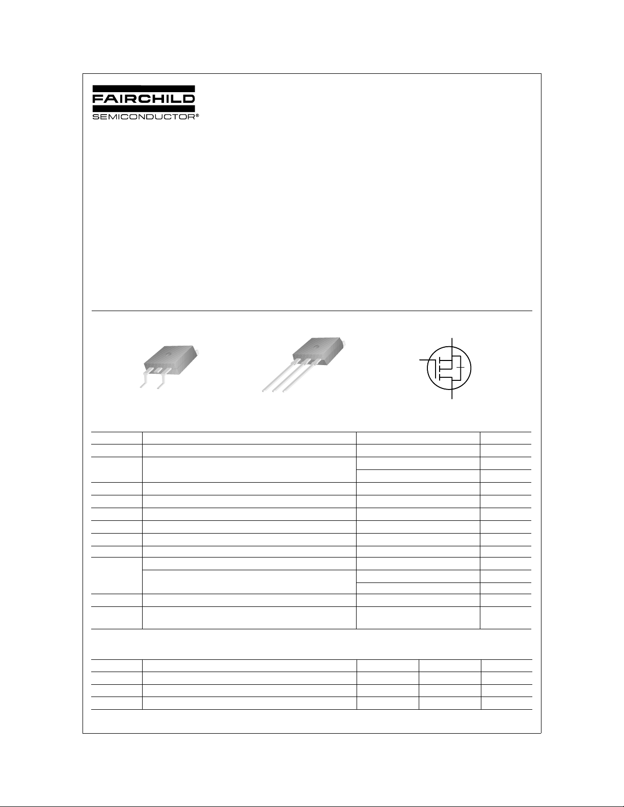
FQB34P10 / FQI34P10
100V P-Channel MOSFET
FQB34P10 / FQI34P10
®
QFET
General Description
These P-Channel enhancement mode power field effect
transistors are produced using Fairchild’s proprietary,
planar stripe, DMOS technology.
This advanced technology has been especially tailored to
minimize on-state resistance, provide superior switching
performance, and withstand high energy pulse in the
avalanche and commutation mode. These devices are well
suited for low voltage applications such as audio amplifier,
Features
• -33.5A, -100V, R
• Low gate charge ( typical 85 nC)
• Low Crss ( typical 170 pF)
• Fast switching
• 100% avalanche tested
• Improved dv/dt capability
• 175°C maximum junction temperature rating
DS(on)
= 0.06Ω @V
= -10 V
GS
high efficiency switching DC/DC converters, and DC motor
control.
S
!!!!
D
GS
D2-PAK
FQB Series
Absolute Maximum Ratings
I2-PAK
GSD
TC = 25°C unless otherw ise noted
FQI Series
G
!!!!
!!!!
!!!!
●●●●
●●●●
●●●●
●●●●
▶▶▶▶
▶▶▶▶
▲▲▲▲
▲▲▲▲
●●●●
●●●●
!!!!
!!!!
D
Symbol Parameter FQB34P10 / FQI34P10 Units
V
DSS
I
D
I
DM
V
GSS
E
AS
I
AR
E
AR
dv/dt Peak Diode Recovery dv/dt
P
D
Drain-Source Voltage -100 V
Drain Current
- Continuous (T
- Continuous (T
Drain Current - Pulsed
= 25°C)
C
= 100°C)
C
(Note 1)
-33.5 A
-23.5 A
-134 A
Gate-Source Voltage ± 25 V
Single Pulsed Avalanche Energy
Avalanche Current
Repetitive Avalanche Energy
Power Dissipation (TA = 25°C) *
Power Dissipation (T
= 25°C)
C
(Note 2)
(Note 1)
(Note 1)
(Note 3)
2200 mJ
-33.5 A
15.5 mJ
-6.0 V/ns
3.75 W
155 W
- Derate above 25°C 1.03 W/°C
, T
T
J
STG
T
L
Operating and Storage Temperature Range -55 to +175 °C
Maximum lead temperature for soldering purposes,
1/8" from case for 5 seconds
300 °C
Thermal Characteristics
Symbol Parameter Typ Max Units
R
θJC
R
θJA
R
θJA
* When mounted on the minimum pad size recommended (PCB Mount)
©2004 Fairchild Semiconductor Corporation
Thermal Resistance, Junction-to-Case -- 0.97 °C/W
Thermal Resistance, Junction-to-Ambient * -- 40 °C/W
Thermal Resistance, Junction-to-Ambient -- 62.5 °C/W
Rev. B, June 2004
FQB34P10 / FQI34P10
Electrical Characteristics
TC = 25°C unless otherwise noted
Symbol Parameter Test Conditions Min Typ Max Unit s
Off Characteristics
BV
DSS
∆BV
DSS
/ ∆T
I
DSS
I
GSSF
I
GSSR
Drain-Source Breakdown Voltage
Breakdown Voltage Temperature
Coefficient
J
Zero Gate Voltage Drain Current
Gate-Body Leakage Current, Forward
Gate-Body Leakage Current, Reverse
= 0 V, I
V
GS
I
= -250 µA, Referenced to 25°C
D
V
= -100 V, VGS = 0 V
DS
= -80 V, TC = 150°C
V
DS
= -25 V, VDS = 0 V
V
GS
= 25 V, VDS = 0 V
V
GS
= -250 µA
D
-100 -- -- V
-- -0.1 -- V/°C
-- -- -1 µA
-- -- -10 µA
-- -- -100 nA
-- -- 100 nA
On Characteristics
V
R
g
FS
GS(th)
DS(on)
Gate Threshold Voltage
Static Drain-Source
On-Resistance
Forward Transconductance
= VGS, I
V
DS
= -10 V, ID = -16.75 A
V
GS
= -40 V, ID = -16.75 A
V
DS
= -250 µA
D
(Note 4)
-2.0 -- -4.0 V
-- 0.049 0.06 Ω
-- 23 -- S
Dynamic Characteristics
C
iss
C
oss
C
rss
Input Capacitance
Output Capacitance -- 730 950 pF
Reverse Transfer Capacitance -- 170 220 pF
= -25 V, VGS = 0 V,
V
DS
f = 1.0 MHz
-- 2240 2910 pF
Switching Characteristics
t
d(on)
t
r
t
d(off)
t
f
Q
Q
Q
g
gs
gd
Turn-On Delay Time
Turn-On Rise Time -- 250 510 ns
Turn-Off Delay Time -- 160 330 ns
Turn-Off Fall Time -- 210 430 ns
Total Gate Charge
Gate-Source Charge -- 15 -- nC
Gate-Drain Charge -- 45 -- nC
= -50 V, ID = -33.5 A,
V
DD
= 25 Ω
R
G
(Note 4, 5)
V
= -80 V, ID = -33.5 A,
DS
V
= -10 V
GS
(Note 4, 5 )
-- 25 60 ns
-- 85 110 nC
Drain-Source Diod e Characteristics and Maximum Ratings
I
S
I
SM
V
SD
t
rr
Q
rr
Notes:
1. Repetitive Rating : Pulse width limited by maximum junction temperature
2. L =mH, I
3. I
≤ -33.5A, di/dt ≤ 300A/µs, VDD ≤ BV
SD
4. Pulse Test : Pulse width ≤ 300µs, Duty cycle ≤ 2%
5. Essentially independent of operating temperature
©2004 Fairchild Semiconductor Corporation
Maximum Continuous Drain-Source Diode Forward Current -- -- -33.5 A
Maximum Pulsed Drain-Source Diode Forward Current -- -- -134 A
= 0 V, IS = -33.5 A
Drain-Source Diode Forward Voltage
Reverse Recovery Time
Reverse Recovery Charge -- 0.88 -- µC
= -33.5A, VDD = -25V, R
AS
= 25 Ω, Starting T
G
Starting TJ = 25°C
DSS,
= 25°C
J
V
GS
= 0 V, IS = -33.5 A,
V
GS
/ dt = 100 A/µs
dI
F
-- -- -4.0 V
-- 160 -- ns
(Note 4)
Rev. B, June 2004
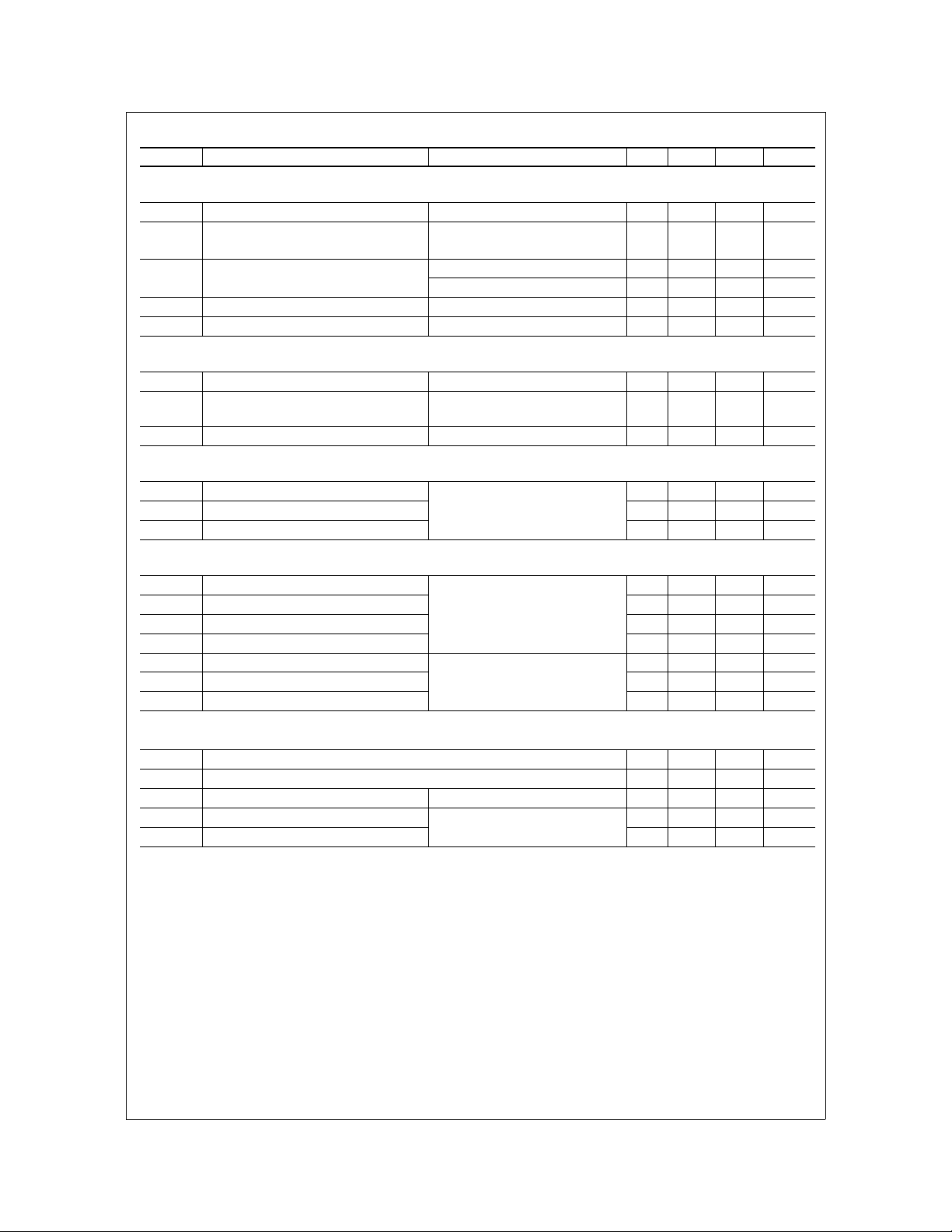
Typical Characteristics
FQB34P10 / FQI34P10
2
V
Top : -15.0 V
-10.0 V
-8.0 V
-7.0 V
-6.5 V
1
-5.5 V
-5.0 V
Bottom : -4.5 V
0
-1
-2
-1
10
GS
Note :
※
1. 250µ s Pulse Test
2. T
= 25
℃
C
0
10
10
10
10
10
, Drain Current [A]
D
-I
10
10
-VDS, Drain-Source Voltage [V]
0.35
0.30
0.25
],
Ω
0.20
[
DS(on)
R
0.15
0.10
Drain-Source On-Resistance
0.05
0.00
0 25 50 75 100 125 150 175 200
VGS = - 10V
VGS = - 20V
※
-ID , Drain Current [A]
1
Note : T
2
10
175
℃
1
10
25
℃
0
10
, Drain Current [A]
D
-I
-1
10
246810
-55
℃
Notes :
※
1. VDS = -40V
2. 250µ s Pulse Test
-VGS , Gate-Source Voltage [V]
Figure 2. Transfer CharacteristicsFigure 1. On-Region Charact er i st ics
2
10
1
10
0
10
25
℃
175
, Reverse Drain Current [A]
= 25
℃
J
-I
℃
DR
-1
10
0.0 0.5 1. 0 1.5 2.0 2. 5 3.0
-VSD , Source- Dr ain Voltage [ V]
Notes :
※
1. VGS = 0V
2. 250µ s Pulse Test
Figure 3. On-Resistance Variation vs.
Drain Current and Gate Voltage
6500
6000
5500
5000
4500
4000
3500
3000
2500
2000
Capacitances [pF]
1500
1000
500
0
-1
10
Figure 5. Capacitance Characteristi cs Fig ure 6. Gate Charge Chara c t eristics
©2004 Fairchild Semiconductor Corporation
C
oss
C
iss
C
rss
0
10
VDS, Drai n-Source Voltage [V]
C
= Cgs + Cgd (Cds = shorted)
iss
= Cds + C
C
oss
gd
C
= C
rss
gd
Notes :
※
1. VGS = 0 V
2. f = 1 MHz
1
10
Figure 4. Body Diode Forward Voltage
Variation vs. Source Current
and Temperature
VDS = -50V
VDS = -80V
VDS = -20V
※
Note : I
= -33.5 A
D
Rev. B, June 2004
12
10
8
6
4
, Gate-Source Voltage [V]
GS
2
-V
0
0 20406080100
QG, Total Gate Charge [nC]
FQB34P10 / FQI34P10
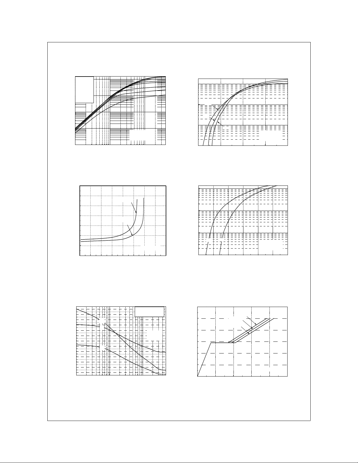
Typical Characteristics
Notes :
※
1. TC = 25 oC
2. T
= 175 oC
J
3. Single Pulse
1
10
DC
1.2
1.1
1.0
, (Normalized)
DSS
-BV
0.9
Drain-So urce Break down Voltage
0.8
-100 -50 0 50 100 150 200
TJ, Juncti on Temperature [oC]
Figure 7. Breakdo w n Voltage Variation
vs. Temperature
Operation in This Ar ea
is Limit ed by R
2
10
1
10
, Drain Current [A]
D
0
-I
10
-1
10
0
10
DS(on)
-VDS, Drai n-Source Voltage [V]
(Continued)
Notes :
※
1. VGS = 0 V
2. I
= -250 µ A
D
100 µs
1 ms
10 ms
2.5
2.0
1.5
, (Normalized)
1.0
DS(ON)
R
0.5
Drain-Source On-Resistance
0.0
-100 -50 0 50 100 150 200
Notes :
※
1. VGS = -10 V
= -16.7 5 A
2. I
D
TJ, Junct ion Temperature [oC]
Figure 8. On-Resistance Variation
vs. Temperature
40
35
30
25
2
10
20
15
, Drain Current [A]
D
-I
10
5
0
25 50 75 100 125 150 175
TC, Case Temperature [ ]
℃
Figure 9. Maximum Safe Operating Area
©2004 Fairchild Semiconductor Corporation
Figure 10. Maximum Drain Current
0
10
D=0.5
0.2
-1
0.1
10
0.05
0.02
0.01
(t), Thermal Response
θ JC
Z
-2
10
-5
10
single pulse
-4
10
-3
10
t1, Square Wave Pulse Duration [sec]
Notes :
※
1. Z
2. Duty Factor , D=t1/t
3. TJM - TC = PDM * Z
-2
10
10
Figure 11. Tr ans ient Ther m al Res pons e Cur ve
vs. Case Temperature
(t) = 0.97 /W M ax.
℃
θ JC
P
DM
-1
2
(t)
θ JC
t
1
t
2
0
10
1
10
Rev. B, June 2004

12V
12V
200nF
200nF
-3mA
-3mA
50KΩ
50KΩ
V
V
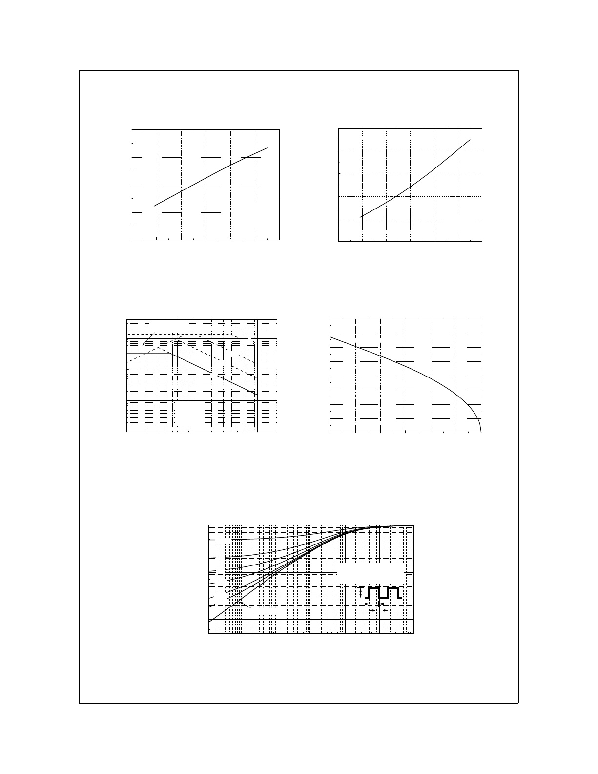
Gate Charge Test Circuit & Waveform
V
V
GS
GS
GS
300nF
300nF
Same Type
Same Type
as DUT
as DUT
DUT
DUT
V
V
DS
DS
GS
-10V
-10V
Resistive Switching Test Circuit & Waveforms
FQB34P10 / FQI34P10
Q
Q
g
g
Q
Q
gs
gs
Q
Q
gd
gd
Charge
Charge
-10V
-10V
-10V
-10V
R
R
L
DUT
DUT
L
V
V
DD
DD
V
V
GS
GS
10%
10%
V
V
DS
DS
V
V
DS
DS
V
V
GS
GS
R
R
G
G
90%
90%
t
t
t
t
d(on)tr
d(on)tr
t
on
on
t
off
off
t
t
d(of f)
d(of f)
t
t
f
f
Unclamped Inductive Switching Test Circuit & Waveforms
BV
BV
DSS
L
LL
V
V
DS
DS
I
IDI
D
D
V
V
DD
BV
BV
DD
I
I
AS
AS
DSS
DSS
R
R
G
G
DUT
DUT
t
t
p
p
V
V
DD
DD
1
1
1
1
----
----
----
----
E
=LI
E
=LI
=LI
E
AS
AS
AS
2
2
2
2
2
2
2
AS
AS
AS
t
t
p
p
I
I
(t)
(t)
D
D
DSS
--------------------
-------------------BV
BV
DSS-VDD
DSS-VDD
Time
Time
V
(t)
V
(t)
DS
DS
©2004 Fairchild Semiconductor Corporation
Rev. B, June 2004

Peak Diode Recovery dv /dt Test Circuit & Waveforms
+
+
V
V
DS
DS
DUT
DUT
I
I
SD
SD
Driver
Driver
R
R
G
G
V
V
GS
GS
_
_
L
LL
Compliment of DUT
Compliment of DUT
(N-Channel)
(N-Channel)
• dv/dt controlled by R
• dv/dt controlled by R
•ISDcontrolled by pulse period
•ISDcontrolled by pulse period
G
G
FQB34P10 / FQI34P10
V
V
DD
DD
V
V
GS
GS
( Driver )
( Driver )
I
I
SD
SD
( DUT )
( DUT )
V
V
DS
DS
( DUT )
( DUT )
Gate Pulse Width
Gate Pulse Width
Gate Pulse Width
--------------------------
--------------------------
--------------------------
D =
D =
D =
Gate Pulse Period
Gate Pulse Period
Gate Pulse Period
Body Diode Reverse Current
Body Diode Reverse Current
I
I
RM
RM
IFM, Body Diode Forward Current
IFM, Body Diode Forward Current
V
V
SD
SD
Body Diode
Body Diode
Forward Voltage Drop
Forward Voltage Drop
Body Diode Recovery dv/dt
Body Diode Recovery dv/dt
di/dt
di/dt
10V
10V
V
V
DD
DD
©2004 Fairchild Semiconductor Corporation
Rev. B, June 2004

Mechanical Dimensions
FQB34P10 / FQI34P10
D2 - PAK
©2004 Fairchild Semiconductor Corporation
Dimensions in Millimeters
Rev. B, June 2004

Mechanical Dimensions
FQB34P10 / FQI34P10
I2 - PAK
©2004 Fairchild Semiconductor Corporation
Dimensions in Millimeters
Rev. B, June 2004

TRADEMARKS
The following are registered and unregistered trademarks Fairchild Semiconductor owns or is authorized to use and is not
intended to be an exhaustive list of all such trademarks.
A
CEx™
ActiveArray™
Bottomless™
CoolFET™
CROSSVOLT™
DOME™
EcoSPARK™
2
E
CMOS™
EnSigna™
FACT™
FACT Quiet Series™
Across the board. Around the world.™
The Power Franchise
Programmable Active Droop™
®
FAST
FASTr™
FPS™
FRFET™
GlobalOptoisolator™
GTO™
HiSeC™
I2C™
i-Lo™
ImpliedDisconnect™
®
ISOPLANAR™
LittleFET™
MICROCOUPLER™
MicroFET™
MicroPak™
MICROWIRE™
MSX™
MSXPro™
OCX™
OCXPro™
OPTOLOGIC
®
OPTOPLANAR™
PACMAN™
POP™
Power247™
PowerSaver™
PowerTrench
QFET
®
®
QS™
QT Optoelectronics™
Quiet Series™
RapidConfigure™
RapidConnect™
µSerDes™
SILENT SWITCHER
SMART START™
SPM™
Stealth™
SuperFET™
SuperSOT™-3
SuperSOT™-6
SuperSOT™-8
SyncFET™
TinyLogic
TINYOPTO™
TruTranslation™
UHC™
UltraFET
®
VCX™
®
®
DISCLAIMER
FAIRCHILD SEMICONDUCTOR RESERVES THE RIGHT TO MAKE CHANGES WITHOUT FURTHER NOTICE TO ANY
PRODUCTS HEREIN TO IMPROVE RELIABILITY, FUNCTION OR DESIGN. FAIRCHILD DOES NOT ASSUME ANY
LIABILITY ARISING OUT OF THE APPLICATION OR USE OF ANY PRODUCT OR CIRCUIT DESCRIBED HEREIN;
NEITHER DOES IT CONVEY ANY LICENSE UNDER ITS PATENT RIGHTS, NOR THE RIGHTS OF OTHERS.
LIFE SUPPORT POLICY
FAIRCHILD’S PRODUCTS ARE NOT AUTHORIZED FOR USE AS CRITICAL COMPONENTS IN LIFE SUPPORT
DEVICES OR SYSTEMS WITHOUT THE EXPRESS WRITTEN APPROVAL OF FAIRCHILD SEMICONDUCTOR
CORPORATION.
As used herein:
1. Life support devices or systems are devices or systems
which, (a) are intended for surgical implant into the body,
or (b) support or sustain life, or (c) whose failure to perform
when properly used in accordance with instructions for use
provided in the labeling, can be reasonably expected to
result in significant injury to the user.
2. A critical component is any component of a life support
device or system whose failure to perform can be
reasonably expected to cause the failure of the life support
device or system, or to affect its safety or effectiveness.
PRODUCT STATUS DEFINITIONS
Definition of Terms
Datasheet Identification Product Status Definition
Advance Information Formative or In
Design
Preliminary First Production This datasheet contains preliminary data, and
No Identification Needed Full Production This datasheet contains final specifications. Fairchild
Obsolete Not In Production This datasheet contains specifications on a product
©2004 Fairchild Semiconductor Corporation
This datasheet contains the design specifications for
product development. Specifications may change in
any manner without notice.
supplementary data will be published at a later date.
Fairchild Semiconductor reserves the right to make
changes at any time without notice in order to improve
design.
Semiconductor reserves the right to make changes at
any time without notice in order to improve design.
that has been discontinued by Fairchild semiconductor.
The datasheet is printed for reference information only.
Rev. I11
 Loading...