

Fairchild FQA36P15 service manual
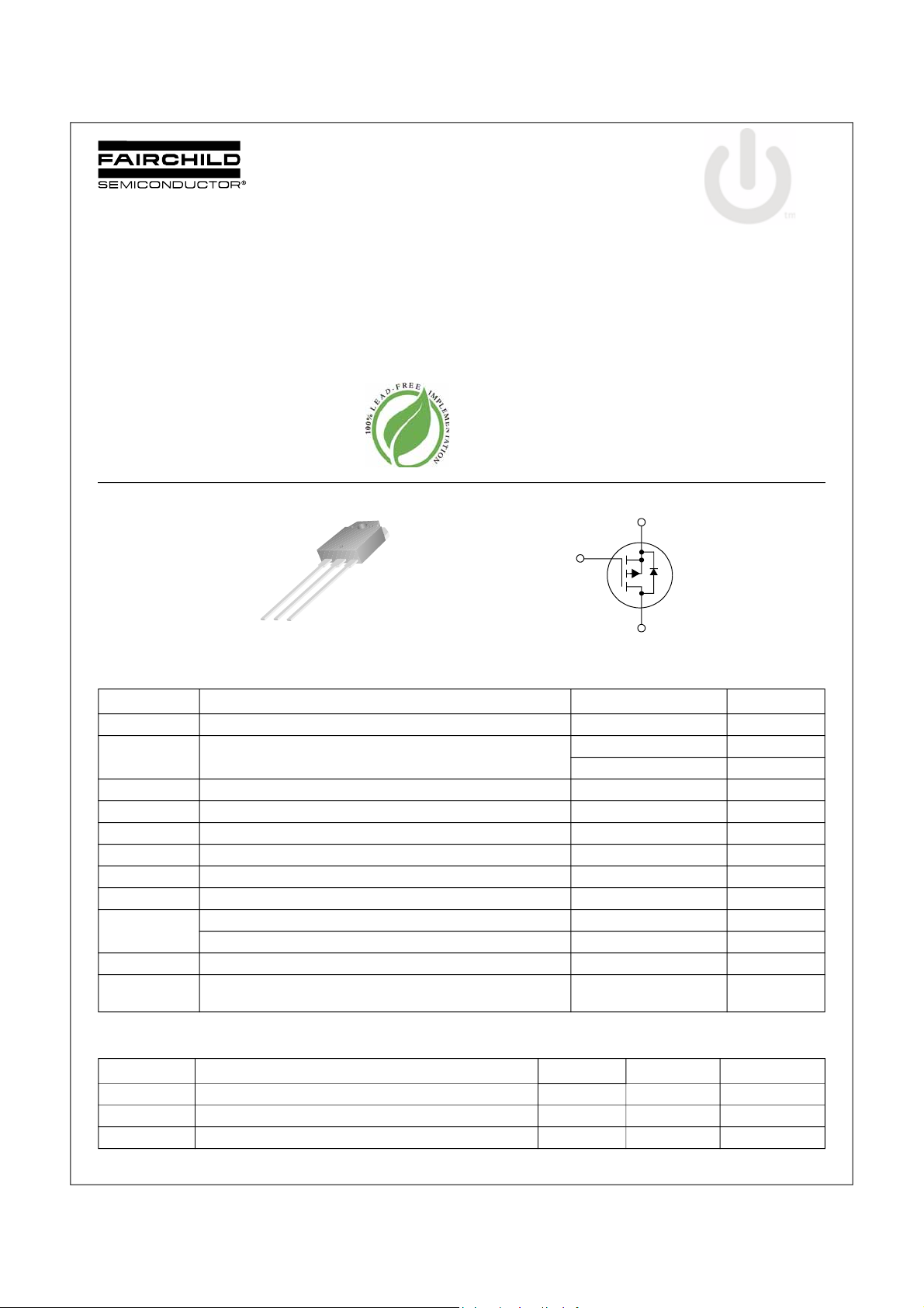
FQA36P15 / FQA36P15_F109
150V P-Channel MOSFET
FQA36P15 / FQA36P15_F109 150V P-Channel MOSFET
September 2010
®
QFET
Features
• -36A, -150V, R
• Low gate charge ( typical 81 nC)
• Low Crss ( typical 110pF)
•Fast switching
• 100% avalanche tested
• Improved dv/dt capability
• 175°C maximum junction temperature rating
= 0.09Ω @VGS = -10 V
DS(on)
GSD
TO-3P
FQA Series
Description
These P-Channel enhancement mode power field effect
transistors are produced using Fairchild’s proprietary, planar
stripe, DMOS technology.
This advanced technology has been especially tailored to
minimize on-state resistance, provide superior switching
performance, and withstand high energy pulse in the avalanche
and commutation mode. These devices are well suited for high
efficient switched mode power supplies, active power factor
correction, electronic lamp ballast based on half bridge
topology.
S
G
D
Absolute Maximum Ratings
Symbol Parameter FQA36P15 Units
V
DSS
I
D
I
DM
V
GSS
E
AS
I
AR
E
AR
dv/dt Peak Diode Recovery dv/dt
P
D
, T
T
J
STG
T
L
Drain-Source Voltage -150 V
Drain Current - Continuous (TC = 25°C) -36 A
- Continuous (T
Drain Current - Pulsed
Gate-Source Voltage ± 30 V
Single Pulsed Avalanche Energy
Avalanche Current
Repetitive Avalanche Energy
Power Dissipation (TC = 25°C) 294 W
- Derate above 25°C 1.96 W/°C
Operating and Storage Temperature Range -55 to +175 °C
Maximum lead temperature for soldering purposes,
1/8" from case for 5 seconds
= 100°C) -25.5 A
C
(Note 1)
(Note 2)
(Note 1)
(Note 1)
(Note 3)
-144 A
1400 mJ
-36 A
29.4 mJ
-5.0 V/ns
300 °C
Thermal Characteristics
Symbol Parameter Typ Max Units
R
θJC
R
θCS
R
θJA
©2010 Fairchild Semiconductor Corporation 1 www.fairchildsemi.com
FQA36P15 / FQA36P15_F109 Rev. B2
Thermal Resistance, Junction-to-Case -- 0.51 °C/W
Thermal Resistance, Case-to-Sink 0.24 -- °C/W
Thermal Resistance, Junction-to-Ambient -- 40 °C/W
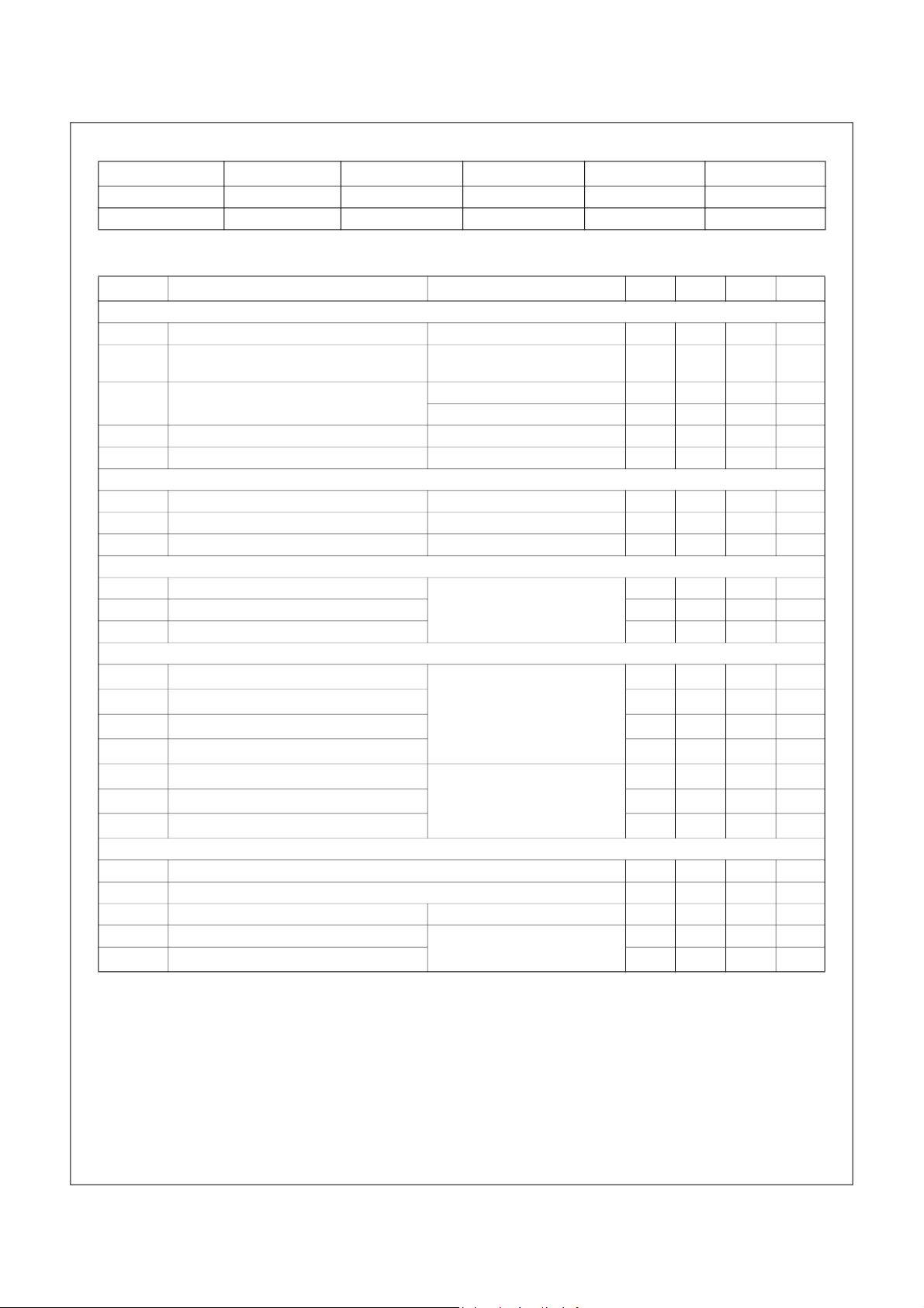
Package Marking and Ordering Information
Device Marking Device Package Reel Size Tape Width Quantity
FQA36P15 FQA36P15 TO-3PN -- -- 30
FQA36P15 FQA36P15_F109 TO-3PN -- -- 30
FQA36P15 / FQA36P15_F109 150V P-Channel MOSFET
Electrical Characteristics T
= 25°C unless otherwise noted
C
Symbol Parameter Test Conditions Min Typ Max Units
Off Characteristics
BV
DSS
∆BV
∆T
J
I
DSS
I
GSSF
I
GSSR
On Characteristics
V
GS(th)
R
DS(on)
g
FS
Dynamic Characteristics
C
iss
C
oss
C
rss
Switching Characteristics
t
d(on)
t
r
t
d(off)
t
f
Q
g
Q
gs
Q
gd
Drain-Source Diode Characteristics and Maximum Ratings
I
S
I
SM
V
SD
t
rr
Q
rr
NOTES:
1. Repetitive Rating : Pulse width limited by maximum junction temperature
2. L = 1.45mH, IAS =-36A, VDD = -50V, RG = 25 Ω, Starting TJ = 25°C
3. ISD ≤ -36A, di/dt ≤300A/µs, VDD ≤ BV
4. Pulse Test : Pulse width ≤ 300µs, Duty cycle ≤ 2%
5. Essentially independent of operating temperature
Drain-Source Breakdown Voltage VGS = 0 V, ID = -250 µA -150 -- -- V
/
DSS
Breakdown Voltage Temperature Coefficient ID = -250 µA, Referenced to 25°C -- -0.13 -- V/°C
Zero Gate Voltage Drain Current VDS = -150 V, VGS = 0 V -- -- -10 µA
= -120 V, TC = 150°C -- -- -100 µA
V
DS
Gate-Body Leakage Current, Forward VGS = -25 V, VDS = 0 V -- -- -100 nA
Gate-Body Leakage Current, Reverse VGS = 25 V, VDS = 0 V -- -- 100 nA
Gate Threshold Voltage VDS = VGS, ID = -250 µA-2.0---4.0V
Static Drain-Source On-Resistance VGS = -10 V, ID = -18A -- 0.076 0.09 Ω
Forward Transconductance VDS = -40 V, ID = -18A (Note 4) -- 19.5 -- S
Input Capacitance VDS = -25 V, VGS = 0 V,
Output Capacitance -- 710 920 pF
Reverse Transfer Capacitance -- 110 140 pF
f = 1.0 MHz
Turn-O n Delay Time VDD = -75 V, ID = -36A,
R
= 25 Ω
Turn-O n Rise Time --
Turn-Off Delay Time --
G
(Note 4, 5)
Turn-Off Fall Time --
Total Gate Charge VDS = -120 V, ID = -36A,
V
= -10 V
Gate-Source Charge --
Gate-Drain Charge --
GS
(Note 4, 5)
-- 2550 3320 pF
--
50 110
350 710
155 320
150 310
--
81 105
19
42
-- nC
-- nC
Maximum Continuous Drain-Source Diode Forward Current -- -- -36 A
Maximum Pulsed Drain-Source Diode Forward Current -- -- -144 A
Drain-Source Diode Forward Voltage VGS = 0 V, IS =-36A -- -- -4.0 V
Reverse Recovery Time VGS = 0 V, IS = -36 A,
dI
/ dt = 100 A/µs (Note 4)
Reverse Recovery Charge -- 1.45 --
Starting TJ = 25°C
DSS,
F
-- 198 -- ns
ns
ns
ns
ns
nC
µC
FQA36P15 / FQA36P15_F109 Rev. B2
2 www.fairchildsemi.com
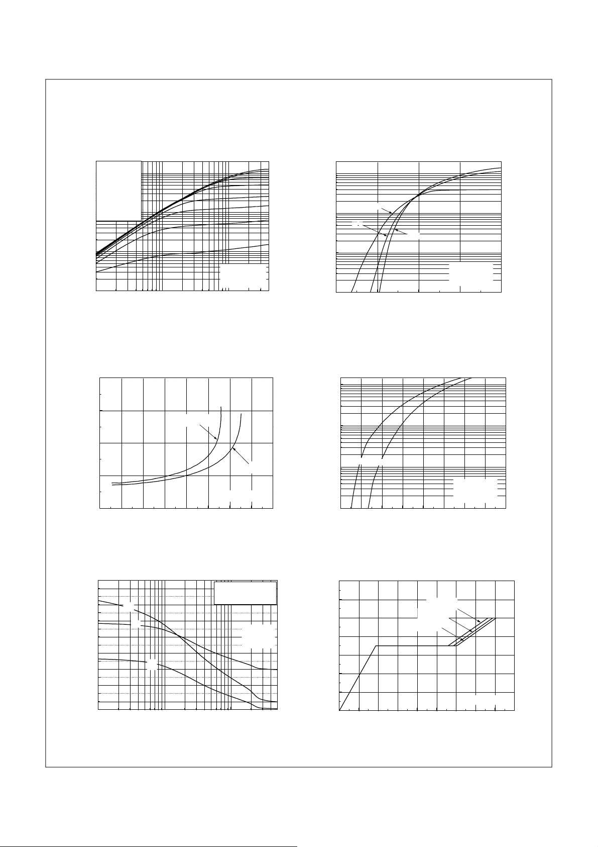
Typical Performance Characteristics
Figure 1. On-Region Characteristics Figure 2. Transfer Characteristics
, Drain Current [A]
D
-I
2
10
1
10
0
10
-1
10
10
V
GS
Top : -15.0 V
-10.0 V
-8.0 V
-7.0 V
-6.0 V
-5.5 V
-5.0 V
Bottom : -4.5 V
-1
0
10
-VDS, Drain-Source Voltage [V]
Notes :※
1. 250µ s Pulse Test
2. T
= 25℃
C
1
10
2
10
1
10
0
10
, Drain Current [A]
D
-I
-1
10
246810
175oC
25oC
-VGS, Gate-Source Volt age [V]
-55oC
Notes :※
1. VDS = -40V
2. 250µ s Pulse Test
FQA36P15 / FQA36P15_F109 150V P-Channel MOSFET
Figure 3. On-Resistance Variation vs. Figure 4. Body Diode Forward Voltage
Drain Current and Gate Voltage Variation vs. Source Current
and Temperatue
0.4
0.3
VGS = -10V
[Ω ],
0.2
DS(ON)
R
0.1
Drain-Source On-Resistance
0.0
0 20 40 60 80 100 120 140 160
-ID, Drain Current [A]
VGS = -20V
Note : T※J = 25℃
2
10
1
10
175℃
0
10
, Reverse Drain Current [A]
DR
-I
-1
10
0.0 0.5 1.0 1.5 2.0 2.5 3.0 3.5 4.0
25℃
-VSD, Source-Drain voltage [V]
Notes :※
1. VGS = 0V
2. 250µ s Pulse Test
Figure 5. Capacitance Characteristics Figure 6. Gate Charge Characteristics
8000
7000
C
6000
5000
4000
3000
Capacitance [pF]
2000
1000
0
10
oss
C
iss
C
rss
-1
0
10
C
= Cgs + Cgd (Cds = shorted)
iss
C
= Cds + C
oss
gd
C
= C
rss
gd
Note ;※
1. VGS = 0 V
2. f = 1 MHz
1
10
-VDS, Drain-Source Voltage [V]
14
12
10
8
6
4
, Gate-Source Voltage [V]
GS
2
-V
0
0 10203040 506070 8090
QG, Total Gate Charge [nC]
VDS = -30V
VDS = -75V
VDS = -120V
Note : I※D = -36A
FQA36P15 / FQA36P15_F109 Rev. B2
3 www.fairchildsemi.com
 Loading...