

FQA13N50CF
500V N-Channel MOSFET
FQA13N50CF 500V N-Channel MOSFET
July 2007
®
FRFET
Features
• 15A, 500V, R
• Low gate charge (typical 43nC)
• Low C
•Fast switching
• 100% avalanche tested
• Improved dv/dt capability
• Fast recovery body diode (typical 100ns)
• RoHS compliant
(typical 20pF)
rss
= 0.48Ω @VGS = 10 V
DS(on)
Description
These N-Channel enhancement mode power field effect
transistors are produced using Fairchild’s proprietary, planar
stripe, DMOS technology.
This advanced technology has been especially tailored to
minimize on-state resistance, provide superior switching
performance, and withstand high energy pulse in the avalanche
and commutation mode. These devices are well suited for high
efficient switched mode power supplies, active power factor
correction, electronic lamp ballast based on half bridge
topology.
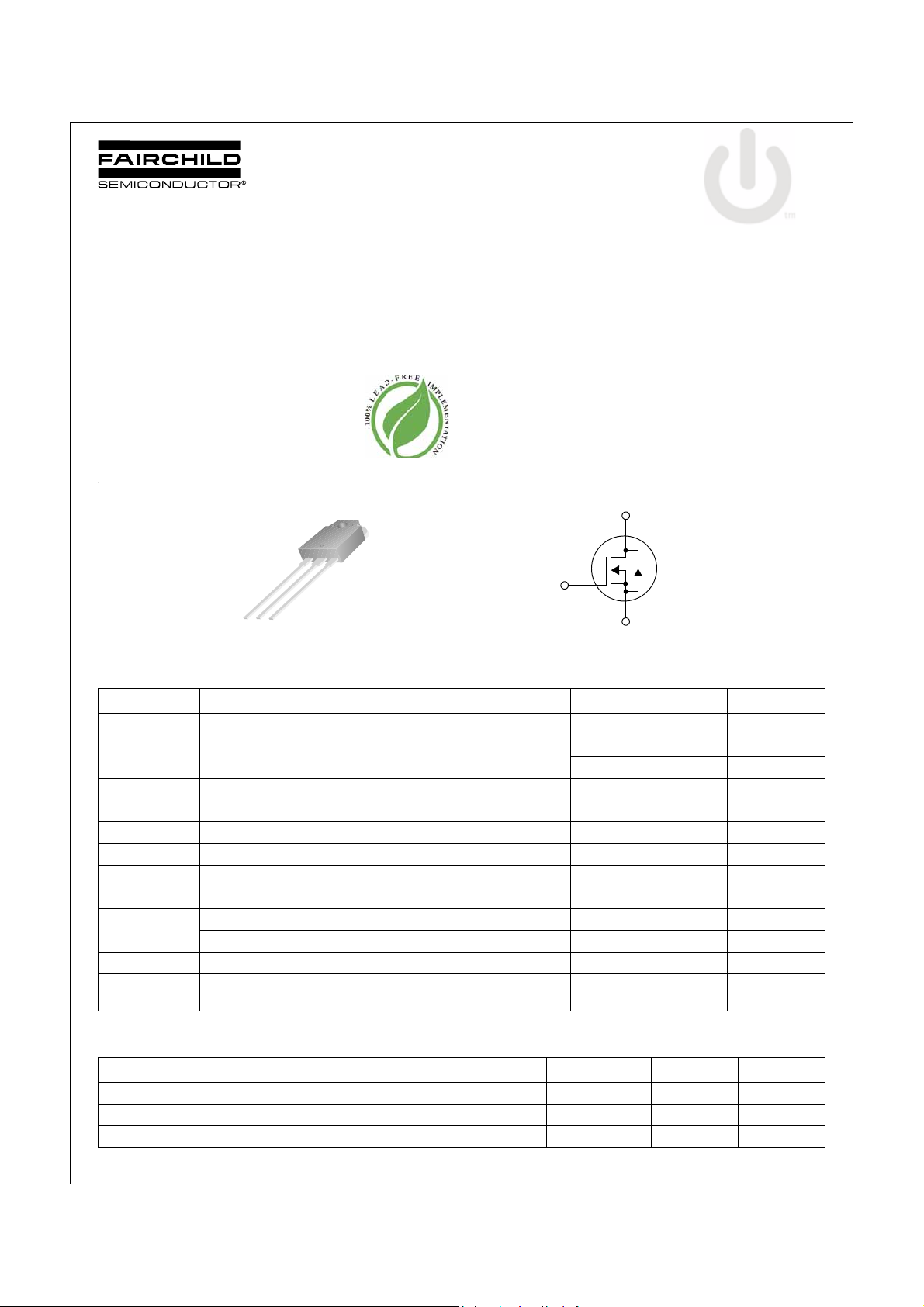
D
G
TO-3PN
GSD
FQA Series
S
Absolute Maximum Ratings
Symbol Parameter FQA13N50CF Units
V
DSS
I
D
I
DM
V
GSS
E
AS
I
AR
E
AR
dv/dt Peak Diode Recovery dv/dt
P
D
T
, T
J
STG
T
L
Drain-Source Voltage 500 V
Drain Current - Continuous (TC = 25°C) 15 A
- Continuous (T
Drain Current - Pulsed
Gate-Source Voltage ± 30 V
Single Pulsed Avalanche Energy
Avalanche Current
Repetitive Avalanche Energy
Power Dissipation (TC = 25°C) 218 W
- Derate above 25°C 1.56 W/°C
Operating and Storage Temperature Range -55 to +150 °C
Maximum lead temperature for soldering purposes,
1/8''"from case for 5 seconds
= 100°C) 9.5 A
C
(Note 1)
(Note 2)
(Note 1)
(Note 1)
(Note 3)
60 A
860 mJ
15 A
21.8 mJ
4.5 V/ns
300 °C
Thermal Characteristics
Symbol Parameter Typ Max Units
R
θJC
R
θJS
R
θJA
©2007 Fairchild Semiconductor Corporation 1 www.fairchildsemi.com
FQA13N50CF Rev. A1
Thermal Resistance, Junction-to-Case -- 0.58 °C/W
Thermal Resistance, Case-to-Sink 0.24 -- °C/W
Thermal Resistance, Junction-to-Ambient -- 40 °C/W
Package Marking and Ordering Information
Device Marking Device Package Reel Size Tape Width Quantity
FQA13N50CF FQA13N50CF TO-3PN -- -- 30
FQA13N50C
F FQA13N50CF_F109 TO-3PN -- -- 30
FQA13N50CF 500V N-Channel MOSFET
Electrical Characteristics T
= 25°C unless otherwise noted
C
Symbol Parameter Test Conditions Min Typ Max Units
Off Characteristics
BV
DSS
∆BV
∆T
J
I
DSS
I
GSSF
I
GSSR
On Characteristics
V
GS(th)
R
DS(on)
g
FS
Dynamic Characteristics
C
iss
C
oss
C
rss
Switching Characteristics
t
d(on)
t
r
t
d(off)
t
f
Q
g
Q
gs
Q
gd
Drain-Source Diode Characteristics and Maximum Ratings
I
S
I
SM
V
SD
t
rr
Q
rr
NOTES:
1. Repetitive Rating : Pulse width limited by maximum junction temperature
2. L = 5.6mH, IAS =15A, VDD = 50V, RG = 25 Ω, Starting TJ = 25°C
3. ISD ≤ 15A, di/dt ≤200A/µs, VDD ≤ BV
4. Pulse Test : Pulse width ≤ 300µs, Duty cycle ≤ 2%
5. Essentially independent of operating temp er ature
Drain-Source Breakdown Voltage VGS = 0 V, ID = 250 µA 500 -- -- V
/
DSS
Breakdown Voltage Temperature Coefficient ID = 250 µA, Referenced to 25°C -- 0.5 -- V/°C
Zero Gate Voltage Drain Current VDS = 500 V, VGS = 0 V -- -- 1 µA
V
= 400 V, TC = 125°C -- -- 10 µA
DS
Gate-Body Leakage Current, Forward VGS = 30 V, VDS = 0 V -- -- 100 nA
Gate-Body Leakage Current, Reverse VGS = -30 V, VDS = 0 V -- -- -100 nA
Gate Threshold Voltage VDS = VGS, ID = 250 µA2.0--4.0V
Static Drain-Source On-Resistance VGS = 10 V, ID = 7.5A -- 0.43 0.48 Ω
Forward Transconductance VDS = 40 V, ID = 7.5 A (Note 4) -- 15 -- S
Input Capacitance VDS = 25 V, VGS = 0 V,
Output Capacitance -- 180 235 pF
Reverse Transfer Capacitance -- 20 25 pF
f = 1.0 MHz
Turn-On Delay Time VDD = 250 V, ID = 15A,
R
= 25 Ω
Turn-On Rise Time -Turn-Off Delay Time --
G
(Note 4, 5)
Turn-Off Fall Time -Total Gate Charge VDS = 400 V, ID = 15A,
= 10 V
V
Gate-Source Charge -Gate-Drain Charge --
GS
(Note 4, 5)
-- 1580 2055 pF
--
25 60
100 210
130 270
100 210
--
43 56
7.5
18.5
-- nC
-- nC
Maximum Continuous Drain-Source Diode Forward Current -- -- 15 A
Maximum Pulsed Drain-Source Diode Forward Current -- -- 60 A
Drain-Source Diode Forward Voltage VGS = 0 V, IS = 15 A -- -- 1.4 V
Reverse Recovery Time VGS = 0 V, IS = 15 A,
/ dt = 100 A/µs (Note 4)
dI
Reverse Recovery Charge -- 0.4 --
Starting TJ = 25°C
DSS,
F
-- 100 -- ns
ns
ns
ns
ns
nC
µC
FQA13N50CF Rev. A1
2 www.fairchildsemi.com

Typical Performance Characteristics
Figure 1. On-Region Characteristics Figure 2. Transfer Characteristics
FQA13N50CF 500V N-Channel MOSFET
-55°C
Notes :
= 40V
1. V
DS
2. 250
µs Pulse Test
, Drain Current [A]
I
10
10
D
10
V
Top : 15.0 V
10.0 V
8.0 V
7.0 V
1
6.0 V
5.5 V
5.0 V
Bottom : 4.5 V
0
-1
-1
10
GS
0
10
VDS, Drain-Source Voltage [V]
Notes :
1. 250us Pulse Test
2. T
= 25°C
C
1
10
1
10
150°C
25°C
0
10
, Drain Current [A]
D
I
-1
10
246810
VGS, Gate-Source Voltage [V]
Figure 3. On-Resistance Variation vs. Figure 4. Body Diode Forward Voltage
Drain Current and Gate Voltage Variation vs. Source Current
and Temperatue
25°C
Notes :
1. V
= 0V
GS
2. 250
µs Pulse Tes t
1.5
VGS = 10V
[Ω],
1.0
DS(ON)
R
VGS = 20V
0.5
Drain-Source On-Resistance
0 5 10 15 20 25 30 35
Note : TJ = 25°C
ID, Drain Current [A]
1
10
0
10
, Reverse Drain Current [A]
DR
I
-1
10
0.2 0.4 0.6 0.8 1.0 1.2 1.4
150°C
VSD, Source-Drain voltage [V]
Figure 5. Capacitance Characteristics Figure 6. Gate Charge Characte ristics
3000
2500
2000
1500
1000
Capacitance [pF]
500
0
-1
10
FQA13N50CF Rev. A1
C
= Cgs + Cgd (Cds = shorted)
iss
C
oss
C
= C
rss
C
iss
C
oss
C
rss
0
10
VDS, Drain -Source Voltag e [V]
= Cds + C
gd
10
gd
Notes ;
1. V
2. f = 1 MHz
1
12
10
8
= 0 V
GS
6
4
, Gate-Source Voltage [V]
2
GS
V
0
0 1020304050
QG, Total Gate Charge [n C]
3 www.fairchildsemi.com
VDS = 100V
VDS = 250V
VDS = 400V
Note : ID = 15A
 Loading...