

Page 1
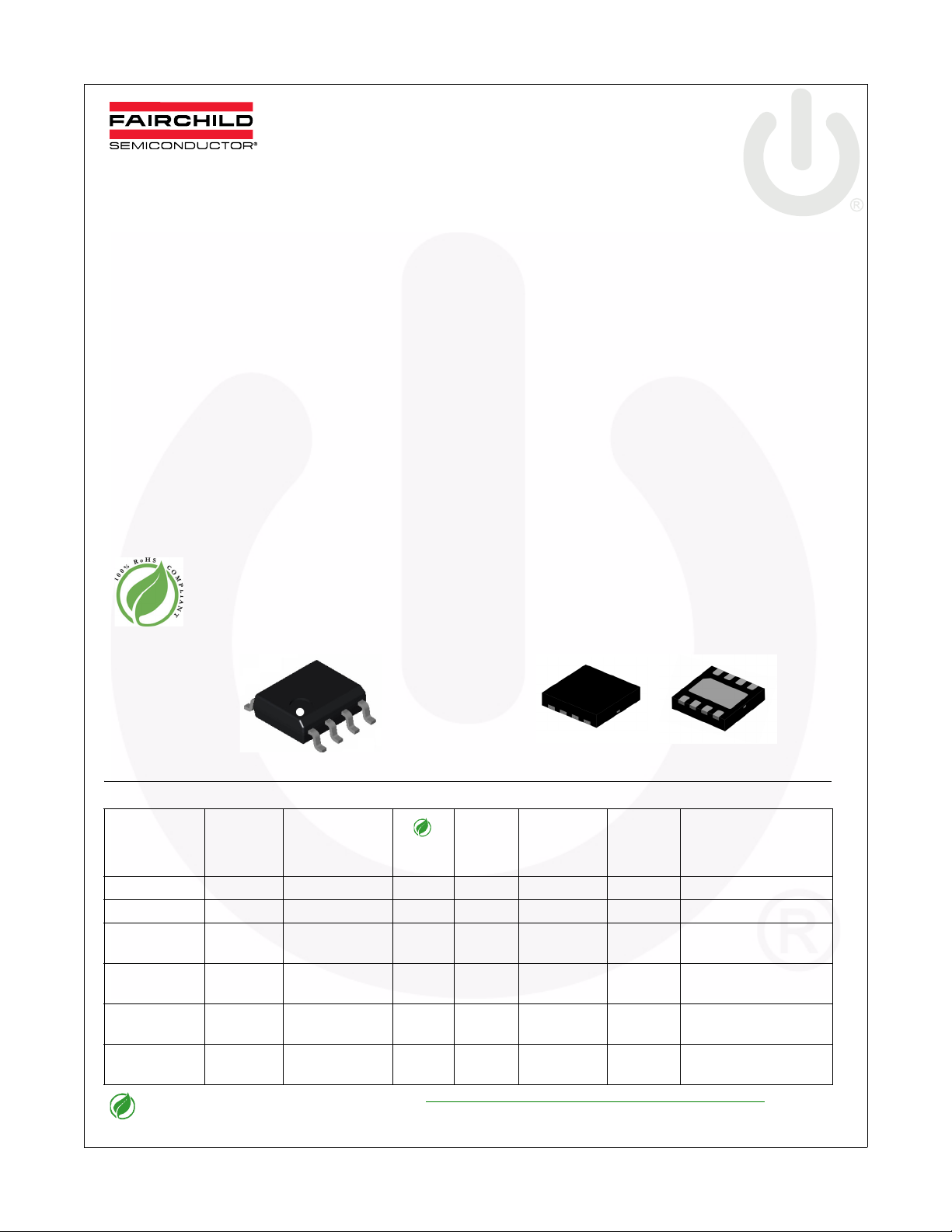
FPF2300/02/03
Dual-Output Current Limit Switch
FPF2300/02/03 — Dual-Output Current Limit Switch
June 2009
Features
! 1.8 to 5.5V Input Voltage Range
! Typical R
! 1.3A Current Limit (Typical)
! Slew Rate Controlled
! Reversed Current Blocking when Disabled
! ESD Protected, Above 4000V HBM
! Independent Thermal Shutdown
! UVLO
! RoHS Compliant
= 75mΩ at IN = 5.5V
ON
Applications
! Notebook Computing
! Peripheral USB Ports
! Networking / USB Based Equiptment
Description
The FPF2300/02/03 are dual-channel load switches of
IntelliMAX™ family. The FPF2300/02/03 consist of dual,
independent, current-limited, slew rate controlled, Pchannel MOSFET power switches. Slew rated turn-on
prevents inrush current from glitching supply rails. The
input voltage range operates from 1.8V to 5.5V to fulfill
today's USB device supply requirements. Switch control
is accomplished by a logic input (ON) capable of
interfacing directly with low-voltage control signal.
For the FPF2302, if the constant current condition persists after 10ms, these parts shut down the switch and
pull the fault signal pin (FLAGB) LOW. The FPF2300 has
an auto-restart feature that turns the switch on again
after 504ms if the ON pin is still active. For the FPF2303,
a current limit condition immediately pulls the fault signal
pin LOW and the part remains in the constant-current
mode until the switch current falls below the current limit.
For the FPF2300 through FPF2303, the current limit is
typically 1.3A for each switch to align with notebook
computing applications. FPF2300/02/03 is available in
both SO8 and MLP 3X3mm 8-lead packages.
Figure 1. 8-Lead SOP Figure 2. 8-Lead MLP (3x3mm)
Ordering Information
Eco
Status
Auto
Restart
ON Pin
Activity
Mode Package
Constant
Current
Constant
Current
8-Lead SO8
8-Lead Molded Leadless Package (MLP)
8-Lead Molded Leadless Package (MLP)
8-Lead Molded Leadless Package (MLP)
Minimum
Part Number
Current
Limit
FPF2300MX 1100mA 10ms RoHS 504ms Active LOW Restart 8-Lead SO8
FPF2302MX 1100mA 10ms RoHS N/A Active LOW Latch Off 8-Lead SO8
FPF2303MX 1100mA 0ms RoHS N/A Active LOW
FPF2300MPX 1100mA 10ms Green 504 Active LOW Restart
FPF2302MPX 1100mA 10ms Green N/A Active LOW Latch Off
FPF2303MPX 1100mA 0ms Green N/A Active LOW
For Fairchild’s definition of Eco Status, please visit: http://www.fairchildsemi.com/company/green/rohs_green.html.
© 2009 Fairchild Semiconductor Corporation www.fairchildsemi.com
FPF2300/02/03 • Rev. 1.1.3
Current Limit
Blanking Time
Page 2
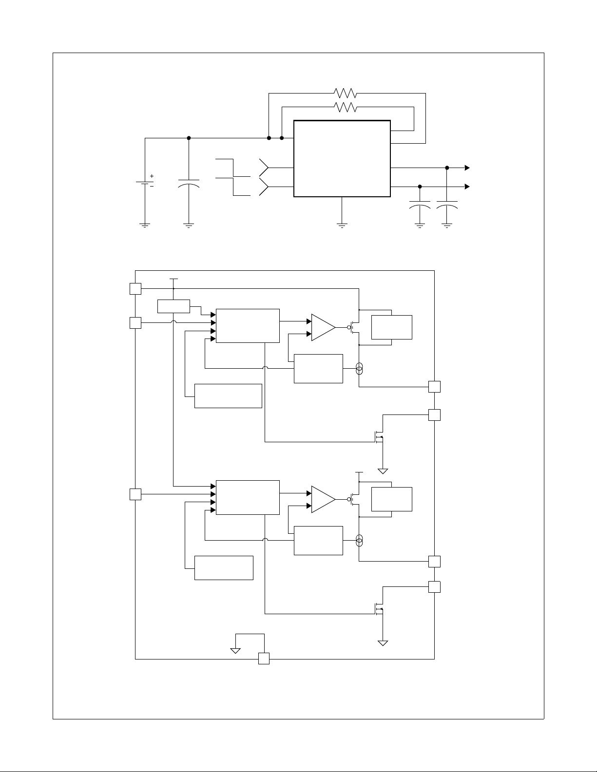
Application Circuit
FPF2300/02/03 — Dual-Output Current Limit Switch
IN = 1.8V-5.5V
C
IN
Functional Block Diagram
IN
UVLO
ONA
PROTECTION A
IN
ONOFF
ONOFF
ONA
ONB
Figure 3. Typical Application
CONTROL
LOGIC A
THERMAL
FPF2300/2/3
GND
CURRENT
LIMIT A
FLAGB(A)
FLAGB(B)
OUTA TO LOAD A
OUTB
REVERSE
CURRENT
BLOCKING
C
OUTB
TO LOAD B
C
OUTA
OUTA
FLAGB(A)
ONB
CONTROL
LOGIC B
THERMAL
PROTECTION B
CURRENT
LIMIT B
REVERSE
CURRENT
BLOCKING
OUTB
FLAGB(B)
GND
Figure 4. Block Diagram
© 2009 Fairchild Semiconductor Corporation www.fairchildsemi.com
FPF2300/02/03 • Rev. 1.1.3 2
Page 3
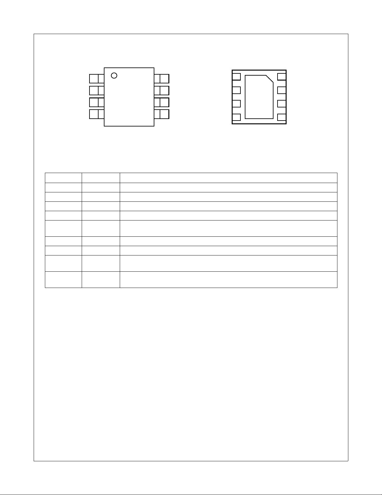
Pin Configuration
FPF2300/02/03 — Dual-Output Current Limit Switch
GND
ONA
ONB
FLAGB(A)
1
IN
2
3
4
SO8
8
OUTA
7
OUTB
6
FLAGB(B)
5
FLAGB(A)
FLAGB(B)
8
OUTA
7
9
63
5
MLP 3X3mm 8-Lead Bottom View
Figure 5. Pin Configurations
Pin Description
Pin # Name Function
1 GND Ground
2 IN Supply Input: Input to the power switch and the supply voltage for the IC.
3 ONA ON / OFF control input of power switch A. Active LOW
4 ONB ON / OFF control input of power switch B. Active LOW
5FLAGB(B)
6 OUTB Switch Output: Output of the power switch B
7 OUTA Switch Output: Output of the power switch A
8FLAGB(A)
9(MLP) Thermal Pad
Fault Output B, Active LO, open drain output which indicates an over supply, UVLO
and thermal shutdown.
Fault Output A, Active LO, open drain output which indicates an over supply, UVLO
and thermal shutdown.
IC Substrate, which can be connected to GND for better thermal performance. Do not
connect to other pins.
GND
1
2
IN
ONAOUTB
4
ONB
© 2009 Fairchild Semiconductor Corporation www.fairchildsemi.com
FPF2300/02/03 • Rev. 1.1.3 3
Page 4
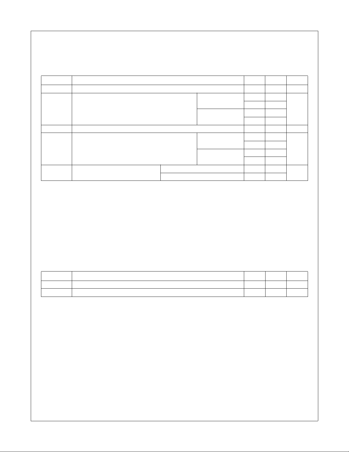
Absolute Maximum Ratings
Stresses exceeding the absolute maximum ratings may damage the device. The device may not function or be operable above the recommended operating conditions and stressing the parts to these levels is not recommended. In addition, extended exposure to stresses above the recommended operating conditions may affect device reliability. The
absolute maximum ratings are stress ratings only
Symbol Parameter Min. Max. Unit
IN, OUTA, OUTB, ONA, ONB, FLAGB(A), FLAGB(B) to GND -0.3 6.0 V
P
T
STG
Θ
JA
ESD Electrostatic Discharge Protection
Notes:
1. Two-layer PCB of 2s0p from JEDEC STD 51-3.
2. Four-layer PBD of 2s0p from JEDEC STD 51-7.
3. Soldered thermal pad on a two-layer PCB without vias based on JEDEC STD 51-3.
4. Soldered thermal pad on a four-layer with two vias connected with GND plane base on JEDEC STD 51-5, 7.
Power Dissipation
D
Storage Temperature -65 +150 °C
Thermal Resistance, Junction-to-Ambient
.
SO8
MLP
SO8
MLP
Human Body Model, JESD22-A114 4000
Charged Device Model, JESD22-C101 2000
0.8
1.4
0.6
2.2
158
92
216
57
(1)
(2)
(3)
(4)
(1)
(2)
(3)
(4)
W
°C/W
V
FPF2300/02/03 — Dual-Output Current Limit Switch
Recommended Operating Range
The Recommended Operating Conditions table defines the conditions for actual device operation. Recommended
operating conditions are specified to ensure optimal performance to the datasheet specifications. Fairchild does not
recommend exceeding them or designing to absolute maximum ratings.
Symbol Parameter Min. Max. Unit
IN Supply Input 1.8 5.5 V
T
Ambient Operating Temperature -40 +85 °C
A
© 2009 Fairchild Semiconductor Corporation www.fairchildsemi.com
FPF2300/02/03 • Rev. 1.1.3 4
Page 5
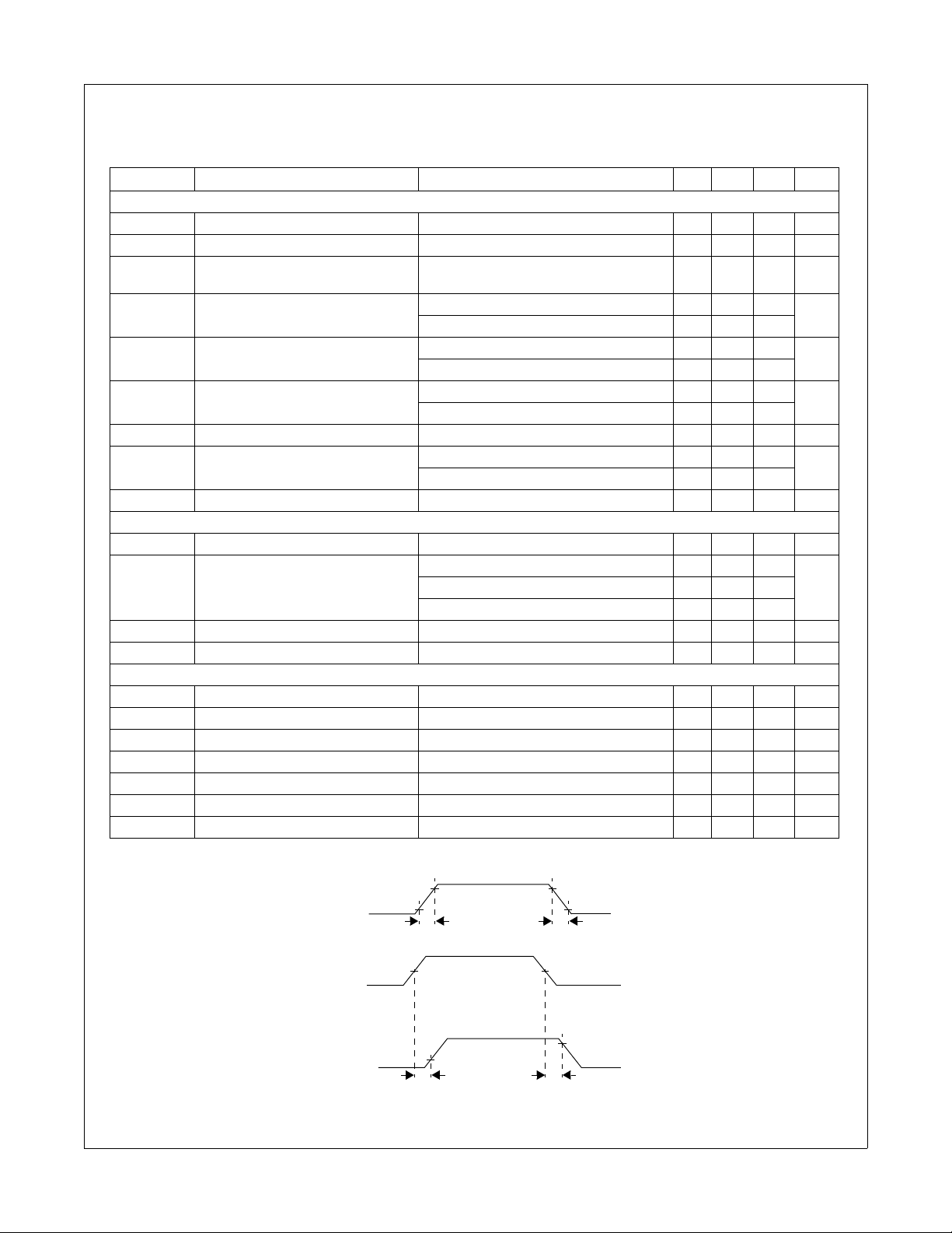
Electrical Characteristics
IN = 1.8 to 5.5V, TA = -40 to +85°C unless otherwise noted. Typical values are at IN = 3.3V and TA = 25°C.
Symbol Parameter Conditions Min. Typ. Max. Units
Basic Operation
V
IN
I
Q
I
SD
R
ON
V
IH
V
IL
I
ON
Protections
I
LIM
TSD Thermal Shutdown
V
UVLO
V
UVLO_HYS
Dynamic
t
ON
t
OFF
t
R
t
BLANK
t
RSTRT_BLANK
t
RSRT
t
CLR
Note:
5. FPF2303 has a 10ms startup FLAGB blanking time when the part is turned on via the ON pin to ensure transient load currents settle.
Operating Voltage 1.8 5.5 V
Quiescent Current IN = 5.5V, V
V
= V
IN Shutdown Current
On Resistance
ON Input Logic High Voltage (ON)
ON Input Logic Low Voltage
ONA
OUTA = OUTB = Short to GND,
IN = 5.5V, I
IN = 5.5V, I
IN = 1.8V 0.8
IN = 5.5V 1.4
IN = 1.8V 0.5
IN = 5.5V 0.9
= V
ONA
= 5.5V, IN = 5.5V
ONB
= 200mA, TA = 25°C 75 140
OUT
= 200mA, TA = -40°C to 85°C 90
OUT
ONB
= 0V, I
= 0mA 52.5 94.5 μA
OUT
3 μA
mΩ
V
V
ON Input Leakage VON = IN or GND -1 1 μA
FLAGB Output Logic Low Voltage
FLAGB Output High Leakage Current IN = V
IN = 5.5V, I
IN = 1.8V, I
ON
Current Limit IN = 3.3V, V
= 1mA 0.1 0.2
SINK
= 1mA 0.15 0.30
SINK
= 5V 1 μA
OUTA
= V
= 3V, TA = 25°C 1.1 1.3 1.5 A
OUTB
V
Shutdown Threshold 140
°CReturn from Shutdown 130
Hysteresis 10
Under-Voltage Shutdown IN Increasing 1.55 1.65 1.75 V
Under-Voltage Shutdown Hysteresis 50 mV
Turn-On Time RL = 500Ω, CL = 0.1μF 113.5 μs
Turn-Off Time RL = 500Ω 6 μs
OUTA, OUTB Rise Time RL = 500Ω, CL = 0.1μF13.5μs
Over-Current Blanking Time FPF2300, FPF2302 5 10 20 ms
Startup FLAGB Blanking Time FPF2303
(5)
51020ms
Auto-Restart Time FPF2300 504 ms
Current Limit Response Time IN = 3.3V, Moderate Over-Current Condition 20 μs
OUT
10%
90%
t
R
90%
10%
t
F
FPF2300/02/03 — Dual-Output Current Limit Switch
ON
OUT
50% 50%
10%
t
DON
t
ON
= tR + t
DON
t
OFF
= tF + t
t
DOFF
90%
DOFF
Figure 6. Timing Diagram
© 2009 Fairchild Semiconductor Corporation www.fairchildsemi.com
FPF2300/02/03 • Rev. 1.1.3 5
Page 6
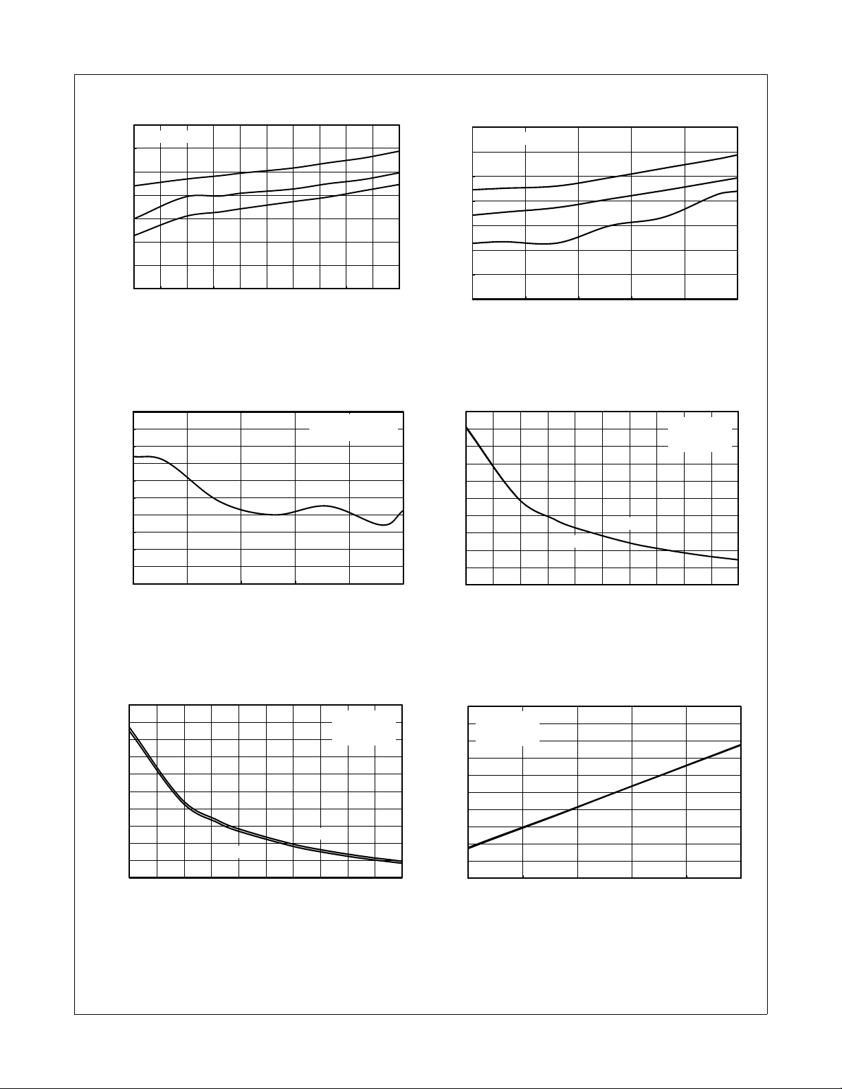
Typical Characteristics
5
)
SUPPLY
CURRENT
(
A)
85°C
C
5
5
)
V
5
5
)
5
A
70.00
ONA = ONB = 0V
60.00
u
50.00
40.00
30.00
20.00
10.00
0.00
1.8 2. 2 2.5 2. 9 3.3 3. 7 4.0 4. 4 4.8 5.1 5.
SUPPLY VOLTAGE (V
25°C
-40°
Figure 7. Quiescent Current vs. Supply Voltage Figure 8. Quiescent Current vs. Temperature
70.00
ONA = ONB = 0V
60.00
50.00
IN = 5.5V
40.00
IN = 3.3V
IN = 1.8V
CURRENT (uA)
Q
I
30.00
20.00
10.00
0.00
-40 -15 10 35 60 8
TJ, JUNCTI ON TEMPERATURE ( °C)
FPF2300/02/03 — Dual-Output Current Limit Switch
5.00
4.50
IN = ONA = ONB = 5.5V
OUT = 0 V
4.00
3.50
3.00
2.50
2.00
1.50
1.00
IN SHUTDOWN CURRENT (uA)
0.50
0.00
-40 -15 10 35 60 8
TJ, J UNCTION TEMPERATURE (° C)
Figure 9. IN Shutdown Current vs. Temperature
160
150
140
130
120
110
100
90
80
ON RESISTANCE (mOhms)
70
R
A
ON
60
1.82.22.52.93.33.74.04.44.85.15.
SUPPLY VOLTAGE (V
R
B
ON
ONA = ONB = 0
I
= 200mA
OUT
T
= 25°C
A
160
150
140
ONA = ONB = 0V
I
= 200mA
OUT
T
= 25°C
A
130
120
110
100
90
80
ON RESISTANCE (mOhms)
R
R
B
ON
A
ON
70
60
1.82.22.52.93.33.74.04.44.85.15.
SUPPLY VOLTAGE (V
Figure 10. RON vs. Supply Voltage (MLP)
100
IN = 5.5V
95
I
= 200mA
OUT
ONA = ONB = 0V
90
85
80
75
70
65
60
ON RESISTANCE ( mOhm)
55
50
-40 -15 10 35 60 8
TJ, JUNCTION TEMPERATURE (°C)
R
B
ON
R
ON
© 2009 Fairchild Semiconductor Corporation www.fairchildsemi.com
Figure 11. RON vs. Temperature (SO8) Figure 12. R
vs. Temperature (MLP)
ON
FPF2300/02/03 • Rev. 1.1.3 6
Page 7

Typical Characteristics
5
A
5
)
L
5
5
5
)
5
A
B
FPF2300/02/03 — Dual-Output Current Limit Switch
90
IN = 5.5V
I
= 200mA
OUT
85
ONA = ONB = 0V
80
75
70
65
60
ON RESISTANCE ( mOhm)
55
50
-40 - 15 10 35 60 8
TJ, JUNCTI ON TEMPERATURE ( °C)
R
B
ON
R
ON
1.5
TA = 25°C
1.3
V
1.0
0.8
0.5
0.3
ON THRESHOLD VOLTAGE (V)
0.0
1.8 2.2 2. 5 2. 9 3.3 3.7 4. 0 4.4 4.8 5. 1 5.
I
V
IH
SUPPLY VOLTAGE (V
Figure 13. RON vs. Temperature (SO8) Figure 14. ON Threshold Voltage vs. Supply Voltage
1.2
IN = 5.5V
1.0
IN = 3.3V
0.8
IN = 1.8V
0.6
0.4
1.2
IN = 5.5V
1.0
0.8
0.6
0.4
IN = 3.3V
IN = 1.8V
0.2
ON THRESHOLD VOLTAGE ( V)
0.0
-40 -15 10 35 60 8
TJ, JUNCTION TEMPERATURE (°C)
Figure 15. ON High Voltage vs. Temperature
1350
TA = 25°C
1340
1330
1320
1310
1300
1290
1280
CURRENT LIMI T (mA)
1270
1260
1250
1.8 2.2 2.5 2.9 3.3 3.7 4.0 4.4 4.8 5.1 5.
ILIM(Typ)A
ILIM(Typ)B
SUPPLY VOLTAGE (V
0.2
ON THRESHOLD VOLTAGE ( V)
0.0
-40 - 15 10 35 60 8
TJ, JUNCTI ON TEMPERATURE ( °C)
Figure 16. ON Low Voltage vs. Temperature
1350
IN = 3.3V
1340
OUTA = OUTB = 3V
ONA = ONB = 0V
1330
1320
1310
1300
1290
1280
CURRENT LIMI T (mA)
1270
1260
1250
-40 - 15 10 35 60 8
ILIM(Typ)
ILIM(Typ)
TJ, JUNCTION TEMPERATURE (°C)
Figure 17. Current Limit vs. Supply Voltage Figure 18. Current Limit vs. Temperature
© 2009 Fairchild Semiconductor Corporation www.fairchildsemi.com
FPF2300/02/03 • Rev. 1.1.3 7
Page 8

Typical Characteristics
5
s
s
5
s
s
5
V
5
)
V
5
V
FPF2300/02/03 — Dual-Output Current Limit Switch
1000
IN = 3.3V
t
DON
100
10
t
DOFF
TURN ON/OFF DELAY TIME (us)
1
-40 - 15 10 35 60 8
TJ, JUNCTION TEMPERATURE (°C)
Figure 19. t
11.0
10.5
10.0
9.5
9.0
8.5
8.0
7.5
OVER CURRENT BLANKING TIME (ms)
7.0
-40 - 15 10 35 60 8
/ t
DON
TJ, J UNCTION TEMPERATURE (° C)
vs. Temperature Figure 20. t
DOFF
FLAGB( B)
FLAGB( A)
R
CL = 0.1 uF
IN = 3.3V
R
FPF2300/ 2
IN = 3.3V
ONA = ONB = 0
= 500 Ohm
L
= 500 Ohm
L
20
18
16
14
12
10
8
6
RISE/FALL TIME (us)
4
2
0
-40 - 15 10 35 60 8
TJ, JUNCTION TEMPERATURE (°C)
RISE
10.0
9.5
9.0
8.5
8.0
7.5
STARTUP FLAGB BLANKI NG TIME ( ms)
7.0
-40 - 15 10 35 60 8
TJ, J UNCTION TEMPERATURE (° C)
t
R
t
F
/ t
vs. Temperature
FAL L
FLAGB( A
FLAGB( B)
IN = 3.3V
R
= 500 Ohm
L
CL = 0.1 uF
IN = 3.3V
R
= 500 Ohm
L
FPF2303
IN = 3.3V
ONA = ONB = 0
620.0
600.0
vs. Temperature
BLANK
FPF2300
IN = 3.3V
ONA = ONB = 0
Figure 22. t
IN
RSTRT_BLANK
vs. TemperatureFigure 21. t
2V/DIV
580.0
560.0
540.0
RESTART TIME (ms)
520.0
500.0
-40 -15 10 35 60 8
TJ, J UNCTION TEMPERATURE (° C)
Figure 23. t
OUTA
OUTB
vs. Temperature Figure 24. tON Response
RSTRT
© 2009 Fairchild Semiconductor Corporation www.fairchildsemi.com
FPF2300/02/03 • Rev. 1.1.3 8
ON
2V/DIV
OUT
2V/DIV
IN = 5V
ON = 3.3V
C
= 0.1μF
OUT
R
= 500Ω
L
200μs/DIV
Page 9

Typical Characteristics
IN
2V/DIV
ON
2V/DIV
t
BLANK
IN = 5V
C
OUT
R
= 2.8Ω
L
FPF2300/02/03 — Dual-Output Current Limit Switch
= 10μF
ON
2V/DIV
IN = 5V
OUT
2V/DIV
ON = 3.3V
C
= 0.1μF
OUT
R
= 500Ω
L
200μs/DIV
ON
2V/DIV
Figure 25. t
t
Response Figure 26. Over-Current Blanking Time (FPF2300/2)
OFF
C
= 10μF
OUT
R
= 3.3Ω
L
START_BLANK
FLAGB
2V/DIV
I
OUT
1A/DIV
OUT
2V/DIV
2ms/DIV
Figure 27. Startup FLAGB Blanking Time (FPF2303)
FLAGB
2V/DIV
I
OUT
1A/DIV
OUT
5V/DIV
2ms/DIV
ON
2V/DIV
t
RSTRT
FLAGB
2V/DIV
I
OUT
1A/DIV
OUT
5V/DIV
100ms/DIV
Figure 28. Auto-Restart Time (FPF2300)
IN = 5V
C
= 10μF
OUT
R
= 2.8Ω
L
IN
5V/DIV
ON
5V/DIV
I
OUT
1A/DIV
C
OUT
= 47μF
C
OUT
= 100μF
C
C
OUT
OUT
IN = 5V
ON = 3.3V
R
= 5Ω
L
= 470μF
= 220μF
200μs/DIV
Figure 29. Current Limit at Startup with
Different Output Capacitor
© 2009 Fairchild Semiconductor Corporation www.fairchildsemi.com
FPF2300/02/03 • Rev. 1.1.3 9
IN
5V/DIV
ON
5V/DIV
OUT
5V/DIV
= 47μFC
OUT
C
= 100μFC
OUT
OUT
= 220μF
OUT
C
200μs/DIV
Figure 30. Output Voltage at Startup with
Different Output Capacitor
IN = 5V
ON = 3.3V
R
= 5Ω
L
= 470μF
Page 10

Typical Characteristics
FPF2300/02/03 — Dual-Output Current Limit Switch
IN
5V/DIV
ON
2V/DIV
IN = 5V
ON = 3.3V
C
OUTA
C
OUTB
R
= RLB = 1Ω
LA
OUTA
2V/DIV
OUTB
2V/DIV
400μs/DIV
Figure 31. Current Limit Response Time Both
Channels are in OC
IN
5V/DIV
ON
5V/DIV
I
OUT
500mA/DIV
IN = 5V
C
OUT
C
= 470μF
L
R
= 5Ω
L
= 100μF
= 100μF
= 47μF
IN
5V/DIV
ON
2V/DIV
FLAGB(A)
2V/DIV
FLAGB(B)
2V/DIV
10ms/DIV
Figure 32. Startup FLAGB Blanking Time
IN
5V/DIV
ON
5V/DIV
I
OUT
2A/DIV
IN = 5V
ON = 3.3V
C
= 100μF
OUTA
C
= 100μF
OUTB
R
= RLB = 1Ω
LA
IN = 5V
C
= 10μF
IN
C
= 100μF
OUT
C
= 47μF
L
OUT
5V/DIV
1ms/DIV
Figure 33. Inrush Response During Capacitive Load
Hot Plug-In Event
OUT
5V/DIV
200μs/DIV
Figure 34. Inrush Response During Capacitive and
Resistive Load Hot Plug-In Event
© 2009 Fairchild Semiconductor Corporation www.fairchildsemi.com
FPF2300/02/03 • Rev. 1.1.3 10
Page 11

Description of Operation
The FPF2300, FPF2302, and FPF2303 are dual-output currentlimit switches designed to meet notebook computer, peripheral
USB port, and point-of-load (POL) application power requirements.
Dual-output current can be used where dual or quad USB ports are
powered by hosts or self-powered hubs. The FPF230X family
offers control and protection while providing optimum operation
current for a safe design practice. The core of each switch is a
typical 75mΩ (IN = 5.5V) P-channel MOSFET and a controller
capable of functioning over an input operating range of 1.8-5.5V.
The FPF230X family offers current limiting, UVLO (under-voltage
lockout), and thermal shutdown protection per each switch. In the
event of an over-current condition, the load switch limits the load to
current limit value. The minimum current limit is set to 1100mA.
On/Off Control
The ON pin is active LOW for FPF2300/2/3 and controls the state
of the switch. Pulling the ON pin continuous to LOW holds the
switch in the ON state. The switch moves into the OFF state when
the ON pin is pulled HIGH or if a fault is encountered. For all
versions, an under-voltage on input voltage or a junction
temperature in excess of 140°C overrides the ON control to turn off
the switch. In addition, excessive currents cause the switch to turn
off in the FPF2300 and FPF2302 after a 10ms blanking time. The
FPF2300 has an auto-restart feature that automatically turns the
switch ON again after 504ms. For the FPF2302, the ON pin must
be toggled to turn on the switch again. The FPF2303 does not turn
off in response to an over-current condition, but remains operating
in a constant-current mode as long as ON is enabled and the
thermal shutdown or UVLO is not activated. The ON pin does not
have a pull-down or pull-up resistor and should not be left floating.
Current Limiting
The current limit ensures that the current through the switch
doesn't exceed a maximum value, while not limiting at less than a
minimum value. FPF230X family has dual-output load switches
being housed in one package. The minimum current at which both
switches start limiting the load current is set to 1100mA. The
FPF2300 and FPF2302 have a blanking time of 10ms (typical),
during which the switch acts as a constant current source. At the
end of the blanking time, the switch is turned off. The FPF2303 has
no current limit blanking period, so it remains in a constant current
state until the ON pin of the affected switch is deactivated or the
thermal shutdown turns off the switch.
Fault Reporting
Over-current, input under-voltage, and over-temperature fault
conditions are signaled out by the FLAGB pin going LOW. A UVLO
fault is reported on both FLAGB(A) and FLAGB(B) simultaneously,
while over-current and over-temperature condition faults are
reported independently. FPF2300 and FPF2302 have a current
fault blanking feature that prevents over-current faults shorter than
the blanking time (t
signal (FLAGB) output.
BLANK(Typ)
If the over-current condition persists beyond the blanking time, the
FPF2300 pulls the FLAGB pin LOW and shuts the switch off. If the
ON pin is kept active, an auto-restart feature releases the FLAGB
pin and turns the switch on again after a 504ms auto-restart time
(t
). If the over-current condition persists beyond the blanking
RSTRT
time, the FPF2302 has a latch-off feature that pulls the FLAGB pin
LOW and shuts the switch off. The switch is kept off and the
FLAGB pin kept LOW until the ON pin is toggled. The FPF2303
responds to an overload condition by immediately pulling the
FLAGB pin LOW and the switch remains in constant current mode
until the output overload condition is removed. The FPF2303 has a
= 10ms) from triggering the fault
startup blanking feature that prevents current faults related to startup transients from triggering the FLAGB output. The startup blanking feature is effective for the first 10ms (typical) following device
turn-on via ON pin.
The FLAGB outputs are two open-drain MOSFETs that require a
pull-up resistor on each FLAGB pin. FLAGB can be pulled HIGH to
a voltage source other than input supply with maximum 5.5V. A
100KΩ pull-up resistor is recommended. When the ON pin is inactive, the FLAGB is disabled to reduce current draw from the supply.
If the FLAGB is not used, the FLAGB can be connected to ground
on the PCB.
.
ON
device wakeup
IN
device wakeup
FLAGB
RISE
TIME
90% V
OUT
I
LOAD
Figure 35. FLAGB Assertion in Under-Voltage Fault
10% V
I
LIMIT
OUT
OUT
ON
VIN
VOUT
ILOAD
Over
current
condt ion
FLAGB
tBLANK
RL*
ILMIT
ILIMIT
tRSTRT
Figure 36. FPF2300 FLAGB Reports While Entering
into an Over-Current Condition
Note:
6. An over-current condition signal loads the output with a
heavy load current larger than I
LIM
value.
FPF2300/02/03 — Dual-Output Current Limit Switch
© 2009 Fairchild Semiconductor Corporation www.fairchildsemi.com
FPF2300/02/03 • Rev. 1.1.3 11
Page 12

FPF2300/02/03 — Dual-Output Current Limit Switch
ON
VIN
VOUT
ILOAD
ILIMIT
Over
current
condtion
FLAGB
Start up
tBLANK
Thermal Shutdown
Device Cools Off
Figure 37. FPF2300 FLAGB While and Over-Current
Condition is Applied
Note:
7. An over-current condition signal loads the output with a
heavy load current larger than I
LIMIT
value.
Under-Voltage Lockout (UVLO)
The under-voltage lockout feature turns off the switch if the
input voltage drops below the under-voltage lockout threshold.
With the ON pin active (ON pin pulled LOW), the input voltage
rising above the under-voltage lockout threshold causes a
controlled turn-on of the switch and limits current overshoot. If a
device is in UVLO condition, both FLAGBs go LOW and indicate
the fault condition. The device detects the UVLO condition when
input voltage goes below UVLO voltage, but remains above
1.3V (typical).
Reverse Current Blocking
Each switch of FPF2300/2/3 has an independent reverse
current blocking feature that protects input source against
current flow from output to input. For a standard USB power
design, this is an important feature that protects the USB host
from being damaged due to reverse current flow on V
activate the reverse current blocking, the switch must be in OFF
BUS
. To
state (ON pins inactivated) so that no current flows from the
output to the input. The FLAGB operation is independent of the
reverse current blocking and does not report a fault condition if
this feature is activated.
Thermal Shutdown
The thermal shutdown protects the device from internally or
externally generated excessive temperatures. Each switch has
an individual thermal shutdown protection function and operates
independently as adjacent switch temperatures increase above
140°C. If one switch is in normal operation and shutdown
protection of second switch is activated, the first channel
continues to operate if the affected channel's heat stays
confined. The over-temperature in one channel can shut down
both switches due to rapidly generated excessive load currents
resulting in very high power dissipation. Generally, a thermally
improved board layout can provide heat sinking and allow heat
to stay confined and not affect the second switch operation.
During an over-temperature condition, the FLAGB is pulled
LOW and the affected switch is turned off. If the temperature of
the die drops below the threshold temperature, the switch
automatically turns on again. To avoid unwanted thermal
oscillations, a 10°C (typical) thermal hysteresis is implemented
between thermal shutdown entry and exit temperatures.
If output of both switches are connected together and an
excessive load current activates thermal protection of both, the
controller can shut down the switches after both FLAGB outputs
go LOW and turn on both channels again. This provides
simultaneous switch turn on. Thermal protection is for device
protection and should not be used as regular operation.
Input Capacitor
To limit the voltage drop on the input supply caused by transient
inrush currents when the switch is turned on into discharged
load capacitors or a short-circuit; an input capacitor, C
recommended between IN and GND. The FPF2310/2/3/3L
, is
IN
features a fast current limit response time of 20μs. An inrush
current (also known as surge current) could occur during the
current limit response time while the switch is responding to an
over-current condition caused by large output capacitors. A
10μF ceramic capacitor, C
the inrush current and prevent input voltage drop at turn on.
Higher values of C
IN
, is required to provide charges for
IN
can be used to further reduce voltage drop.
Output Capacitor
A 0.1μF to 1μF capacitor, C
OUT and GND pins. This capacitor prevents parasitic board
inductances from forcing output voltage below GND when the
switch turns off. This capacitor should have a low dissipation
factor. An X7R MLCC (Multilayer Ceramic Chip) capacitors is
recommended.
For the FPF2300 and FPF2302, the total output capacitance
needs to be kept below a maximum value, C
prevent the part from registering an over-current condition
beyond the blanking time and shutdown. The maximum output
capacitance for a giving input voltage can be determined from
the following:
C
OUT(MAX)
For example, in a 5V application, C
as:
C
OUT(MAX)(IN = 5V)
, should be placed between the
OUT
I
x t
=
LIM(MIN)
BLANK(MIN)
V
IN
OUT(MAX)
can be determined
1.1A x 5ms
=
1.1mF
=
5
OUT(MAX)
, to
(1)
(2)
© 2009 Fairchild Semiconductor Corporation www.fairchildsemi.com
FPF2300/02/03 • Rev. 1.1.3 12
Page 13

Application Information
FPF2300/02/03 — Dual-Output Current Limit Switch
Host
IN
5V
1μF
FPF230X is designed to simplify USB port power design based
on self-powering USB host/hub applications. A self-powering
USB port is powered by a local 5V power supply, not by an
upstream port. Each port should supply at least 500mA to each
downstream function based on USB 2.0 specification. Implementation can depend on the number of USB ports and current
OFF ON ONA
OFF ON ONB OUTB
Figure 38. Self Powered 4-Port USB Hub Using a Single FPF230X
10KΩ
10KΩ
FLAGB(A)
FLAGB(B)
33μF
33μF
Downstream
USB Port
Downstream
USB Port
FPF2300/2/3
OUTA
GND
33μF
33μF
capability per port required in actual power designs. FPF230X
has 1.1A minimum current limit per output, which can cover two
ports, as shown in Figure 38. Four USB ports can be implemented with a single FPF230X part and current limiting is provided based on a two-port basis for a cost-effective solution.
10KΩ
10KΩ
Downstream
USB Port
Downstream
USB Port
Host
5V
1μF
1μF
Figure 39. Individual Port Power Management for Self-Powered 4-Port USB Hub
In Figure 39, each USB port is connected with each output.
Four USB ports can be implemented with two FPF230X parts.
Current limiting and control are provided based on a single port.
OFF ON ONA
OFF ON ONB OUTB
OFF ON ONA
OFF ON ONB OUTB
IN
FLAGB(A)
FLAGB(B)
33μF
Downstream
USB Port
FPF2300/2/3
OUTA
Downstream
USB Port
Downstream
USB Port
IN
GND
10KΩ
10KΩ
FLAGB(A)
FLAGB(B)
33μF
33μF
FPF2300/2/3
OUTA
GND
33μF
Current capability per port has more headroom; up to a minimum of 1.1A per port.
Downstream
USB Port
© 2009 Fairchild Semiconductor Corporation www.fairchildsemi.com
FPF2300/02/03 • Rev. 1.1.3 13
Page 14

10KΩ
10KΩ
FPF2300/02/03 — Dual-Output Current Limit Switch
Host
IN
5V
1μF
High current, over 2A, is sometimes required to supply enough
power to downstream functions. As shown in Figure 40, a 2.2A
OFF ON ONA
OFF ON ONB OUTB
Figure 40. Self-Powered USB Port for High Current Demand
Power Dissipation
During normal operation as a switch, the power dissipation of
the device is small and has little effect on the operating
temperature of the part. The maximum power dissipation for
both switches while the switch is in normal operation occurs just
before both channels enter into current limit. This may be
calculated using the formula:
P
D_MAX(Normal Operation)
For example, for a 5V application, maximum normal operation
power loss while both switches delivering output current up to
1.1A, can be calculated as:
P
D_MAX(Normal Operation)(IN = 5V)
The maximum junction temperature should be limited to 125°C
under normal operation. Junction temperature can be calculated using the formula below:
T
= PD x R
J
θJA
where:
T
is junction temperature;
J
P
is power dissipation across the switch;
D
R
is thermal resistance junction to ambient of the package;
θJA
T
is ambient temperature.
A
For the example, T
with T
=25°C while both switches are delivering up to 1.1A is
A
calculated as:
T
J(MAX)(NormalOperation)
= P
D_MAX(Normal Operation)(IN = 5V)
= 78.4°C
= 2 x (I
LIM(MIN)
= 2 x (1.1)2 x 0.14
=
+ T
A
J(MAX)(Normal operation)
)2 x R
ON(MAX)
(3)
(4)
338mW
(5)
for an SO8 package
x 125 + 25
(6)
FLAGB(A)
FLAGB(B)
FPF2300/2/3
OUTA
GND
33μF
minimum load current can be achieved by tying dual outputs
together.
If the part goes into current limit, the maximum power
dissipation occurs when the output of switch is shorted to
ground. For the FPF2300 the power dissipation scales with the
auto-restart time, t
t
. In this case, the maximum power dissipated for the
BLANK
FPF2300 is::
P
D_MAX(CurrentLimit)
, and the over-current blanking time,
RSTRT
t
t
BLANK
BLANK
+ t
=
2 x x IN
which results in:
P
D_MAX(CurrentLimit)
=
10 + 504
10
2 x
Note that this is below the maximum package power dissipation
and the thermal shutdown feature protection provides additional
safety to protect the part from damage due to excessive
heating. The junction temperature is only able to increase to the
thermal shutdown threshold. Once this temperature has been
reached, toggling ON has no affect until the junction
temperature drops below the thermal shutdown exit
temperature. For the FPF2303, a short on both outputs causes
both switches to operate in a constant current state and
dissipate a worst-case power of:
MAX
= 2 x IN
(MAX)
x I
LIM(MAX)
= 2 x 5.5 x1.5 = 16.5 W
As both FPF2303 outputs are connected to GND.
This power dissipation is significant and activates both thermal
shutdown blocks and the part can cycle in and out of thermal
shutdown as long as the ON pin is activated (pulled LOW) and
the output short is present.
Downstream
USB Port
RSTRT
(MAX)
x 5.5 x 1.5 = 321mW
x I
LIM(MAX)
(7)
(8)
(9)P
© 2009 Fairchild Semiconductor Corporation www.fairchildsemi.com
FPF2300/02/03 • Rev. 1.1.3 14
Page 15

PCB Layout Recommendations
For the best performance, all traces should be as short as
possible. To be most effective, the input and output capacitors
should be placed close to the device to minimize the effects that
parasitic trace inductances may have on normal and shortcircuit operation. Using wide traces for IN, OUTs, and GND pins
helps minimize parasitic electrical effects and the case-toambient thermal impedance.
Improving Thermal Performance
Improper layout could result in higher junction temperature and
triggering the thermal shutdown protection feature. This concern
is particularly significant for the FPF2303, where both channels
operate in constant current mode in the overload conditions and
during fault condition the outputs are shorted, resulting in large
voltage drop across switches. In this case, power dissipation of
the switch (P
maximum absolute power dissipation of part.
The following techniques improve the thermal performance of
this family of devices. These techniques are listed in order of
the significance of impact.
1. Thermal performance of the load switch can be improved
by connecting the DAP (Die Attach Pad) of MLP 3x3mm
package to the GND plane of the PCB.
2. Embedding two exposed through-hole vias into the DAP
(pin 9) provides a path for heat to transfer to the back GND
plane of the PCB. A drill size of round, 15 mils (0.4mm),
with 1-ounce copper plating is recommended to create
appropriate solder reflow. A smaller size hole prevents the
solder from penetrating into the via, resulting in device liftup. Similarly, a larger via hole consumes excessive solder
and may result in voiding of the DAP.
= (VIN - V
D
OUT
) x I
) could exceed the
LIM(MAX)
FPF2300/02/03 — Dual-Output Current Limit Switch
Figure 42. Proper Layout of Output and Ground
Copper Area
15mil
25mil
Figure 41. Two Through-Hole Open Vias Embedded
in DAP
3. The IN, OUTs, and GND pins dissipate most of the heat
generated during a high load current condition. Figure 42
illustrates a proper layout for devices in MLP 3x3mm
packages. IN, OUTs, and GND pins are connected to
adequate copper so heat may be transferred as efficiently
as possible out of the device. The low-power FLAGB and
ON pin traces may be laid out diagonally from the device to
maximize the area available to the ground pad. Placing the
input and output capacitors as close to the device as
possible also contributes to heat dissipation, particularly
during high load currents.
© 2009 Fairchild Semiconductor Corporation www.fairchildsemi.com
FPF2300/02/03 • Rev. 1.1.3 15
Page 16

FPF230X Evaluation Board
The FPF230X evaluation board has components and circuitry to
demonstrate FPF2300/2/3 load switch functions and features,
accommodating both the MLP 3x3mm and SO8 packages. The
state of the each channel can be configured using J1 and J2
jumpers. In addition, both channels can be controlled by ONA
and ONB test pints. Thermal performance of the board is
improved using techniques in the layout recommendations
section. R3 and R4 resistors are used on the board to sink a
light load current when switches are activated.
FPF2300/02/03 — Dual-Output Current Limit Switch
Figure 44. Bottom and ASB Layers
Figure 43. Top, SST and AST Layers
(MLP 3x3mm and SO8)
Figure 45. Zoom-In to Top Layer
Releated Resources
FPF2300/02/03 Evaluation Board User Guide; Power Switch for USB Applications
© 2009 Fairchild Semiconductor Corporation www.fairchildsemi.com
FPF2300/02/03 • Rev. 1.1.3 16
Page 17

Dimensional Outline and Pad Layout
FPF2300/02/03 — Dual-Output Current Limit Switch
Figure 46. 8-Lead SO8 Package
Package drawings are provided as a service to customers considering Fairchild components. Drawings may change in any manner
without notice. Please note the revision and/or date on the drawing and contact a Fairchild Semiconductor representative to verify or
obtain the most recent revision. Package specifications do not expand the terms of Fairchild’s worldwide terms and conditions,
specifically the warranty therein, which covers Fairchild products.
Always visit Fairchild Semiconductor’s online packaging area for the most recent package drawings:
http://www.fairchildsemi.com/packaging/
© 2009 Fairchild Semiconductor Corporation www.fairchildsemi.com
FPF2300/02/03 • Rev. 1.1.3 17
.
Page 18

Dimensional Outline and Pad Layout
FPF2300/02/03 — Dual-Output Current Limit Switch
Figure 47. 8-Lead Molded Leadless Package (MLP)
Package drawings are provided as a service to customers considering Fairchild components. Drawings may change in any manner
without notice. Please note the revision and/or date on the drawing and contact a Fairchild Semiconductor representative to verify or
obtain the most recent revision. Package specifications do not expand the terms of Fairchild’s worldwide terms and conditions,
specifically the warranty therein, which covers Fairchild products.
Always visit Fairchild Semiconductor’s online packaging area for the most recent package drawings:
http://www.fairchildsemi.com/packaging/
© 2009 Fairchild Semiconductor Corporation www.fairchildsemi.com
FPF2300/02/03 • Rev. 1.1.3 18
.
Page 19

TRADEMARKS
The following includes registered and unregistered trademarks and service marks, owned by Fairchild Semiconductor and/or its global subsidianries, and is
not intended to be an exhaustive list of all such trademarks.
Auto-SPM™
Build it Now™
CorePLUS™
CorePOWER™
CROSSVOLT™
CTL™
Current Transfer Logic™
EcoSPARK
EfficentMax™
EZSWITCH™*
®
™*
®
Fairchild
Fairchild Semiconductor
FACT Quiet Series™
®
FACT
®
FAST
FastvCore™
FETBench™
FlashWriter
®
*
FPS™
F-PFS™
®
FRFET
Global Power Resource
Green FPS™
Green FPS™ e-Series™
Gmax™
GTO™
IntelliMAX™
ISOPLANAR™
MegaBuck™
MICROCOUPLER™
MicroFET™
MicroPak™
MillerDrive™
®
MotionMax™
Motion-SPM™
OPTOLOGIC
OPTOPLANAR
®
®
SM
®
PDP SPM™
PowerTrench
PowerXS™
Programmable Active Droop™
QFET
QS™
Quiet Series™
RapidConfigure™
Saving our world, 1mW/W/kW at a time™
SmartMax™
SMART START™
SPM
STEALTH™
SuperFET™
SuperSOT™-3
SuperSOT™-6
SuperSOT™-8
SupreMOS™
SyncFET™
Sync-Lock™
Power-SPM™
®
®
™
®
®
*
The Power Franchise
TinyBoost™
TinyBuck™
®
TinyLogic
TINYOPTO™
TinyPower™
TinyPWM™
TinyWire™
TriFault Detect™
TRUECURRENT™*
μSerDes™
®
UHC
Ultra FRFET™
UniFET™
VCX™
VisualMax™
XS™
®
* Trademarks of System General Corporation, used under license by Fairchild Semiconductor.
DISCLAIMER
FAIRCHILD SEMICONDUCTOR RESERVES THE RIGHT TO MAKE CHANGES WITHOUT FURTHER NOTICE TO ANY PRODUCTS HEREIN TO IMPROVE
RELIABILITY, FUNCTION, OR DESIGN. FAIRCHILD DOES NOT ASSUME ANY LIABILITY ARISING OUT OF THE APPLICATION OR USE OF ANY
PRODUCT OR CIRCUIT DESCRIBED HEREIN; NEITHER DOES IT CONVEY ANY LICENSE UNDER ITS PATENT RIGHTS, NOR THE RIGHTS OF OTHERS.
THESE SPECIFICATIONS DO NOT EXPAND THE TERMS OF FAIRCHILD°ØS WORLDWIDE TERMS AND CONDITIONS, SPECIFICALLY THE WARRANTY
THEREIN, WHICH COVERS THESE PRODUCTS.
LIFE SUPPORT POLICY
FAIRCHILD’S PRODUCTS ARE NOT AUTHORIZED FOR USE AS CRITICAL COMPONENTS IN LIFE SUPPORT DEVICES OR SYSTEMS WITHOUT THE
EXPRESS WRITTEN APPROVAL OF FAIRCHILD SEMICONDUCTOR CORPORATION.
As used herein:
1. Life support devices or systems are devices or systems which, (a) are
intended for surgical implant into the body or (b) support or sustain life,
and (c) whose failure to perform when properly used in accordance with
instructions for use provided in the labeling, can be reasonably
expected to result in a significant injury of the user.
2. A critical component in any component of a life support, device, or
system whose failure to perform can be reasonably expected to cause
the failure of the life support device or system, or to affect its safety or
effectiveness.
ANTI-COUNTERFEITING POLICY
Fairchild Semiconductor Corporation's Anti-Counterfeiting Policy. Fairchild's Anti-Counterfeiting Policy is also stated on our external website,
www.fairchildsemi.com, under Sales Support.
Counterfeiting of semiconductor parts is a growing problem in the industry. All manufacturers of semiconductor products are experiencing counterfeiting of
their parts. Customers who inadvertently purchase counterfeit parts experience many problems such as loss of brand reputation, substandard performance,
failed applications, and increased cost of production and manufacturing delays. Fairchild is taking strong measures to protect ourselves and our customers
from the proliferation of counterfeit parts. Fairchild strongly encourages customers to purchase Fairchild parts either directly from Fairchild or from Authorized
Fairchild Distributors who are listed by country on our web page cited above. Products customers buy either from Fairchild directly or from Authorized Fairchild
Distributors are genuine parts, have full traceability, meet Fairchild's quality standards for handling and storage and provide access to Fairchild's full range of
up-to-date technical and product information. Fairchild and our Authorized Distributors will stand behind all warranties and will appropriately address any
warranty issues that may arise. Fairchild will not provide any warranty coverage or other assistance for parts bought from Unauthorized Sources. Fairchild is
committed to combat this global problem and encourage our customers to do their part in stopping this practice by buying direct or from authorized distributors.
FPF2300/02/03 — Dual-Output Current Limit Switch
PRODUCT STATUS DEFINITIONS
Definition of Terms
Datasheet Identification Product Status Definition
Advance Information Formative / In Design
Preliminary First Production
No Identification Needed Full Production
Obsolete Not In Production
Datasheet contains the design specifications for product development. Specifications may change
in any manner without notice.
Datasheet contains preliminary data; supplementary data will be published at a later date. Fairchild
Semiconductor reserves the right to make changes at any time without notice to improve design.
Datasheet contains final specifications. Fairchild Semiconductor reserves the right to make
changes at any time without notice to improve the design.
Datasheet contains specifications on a product that is discontinued by Fairchild Semiconductor.
The datasheet is for reference information only.
Rev. I40
© 2009 Fairchild Semiconductor Corporation www.fairchildsemi.com
FPF2300/02/03 • Rev. 1.1.3 19
 Loading...