FPF1107 / FPF1108
Advance Load Management Switch
FPF1107 / FPF1108 — Advance Load Management Switch
November 2009
Features
1.2V to 4V Input Voltage Operating Range
Typical R
- 35mΩ at V
- 55mΩ at V
- 85mΩ at V
Slew Rate Control with t
DS(ON)
:
=3.3V
IN
=1.8V
IN
=1.2V
IN
: 130µs
R
Output Discharge Function on FPF1108
Low <1µA Quiescent Current at V
ON=VIN
ESD Protected: Above 4000V HBM, 2000V CDM
GPIO/CMOS-Compatible Enable Circuitry
Applications
Mobile Devices and Smart Phones
Portable Media Devices
Digital Cameras
Advanced Notebook, UMPC, MID
Portable Medical Devices
GPS and Navigation Equipment
Description
The FPF1107/08 are low RDS P-channel MOSFET load
switches of the IntelliMAX™ family. Integrated slew-rate
control prevents inrush current from glitch supply rails
with capacitive loads common in power applications.
The input voltage range operates from 1.2V to 4V to
fulfill today's lowest ultra-portable device supply
requirements. Switch control is by a logic input (ON-pin)
capable of interfacing directly with low-voltage CMOS
control signals and GPIOs in embedded processors.
Ordering Information
Part
Number
FPF1107 QC 55mΩ CMOS NA
FPF1108 QD 55mΩ CMOS 65Ω
For Fairchild’s definition of Eco Status, please visit: http://www.fairchildsemi.com/company/green/rohs_green.html.
© 2009 Fairchild Semiconductor Corporation www.fairchildsemi.com
FPF1107 / FPF1108 • Rev. 1.0.1
Part
Marking
Switch
(Typical)
At 1.8V
IN
Input
Buffer
Output
Discharge
ON Pin
Activity
Active
HIGH
Active
HIGH
Eco
t
R
Status
130µs Green
130µs Green
Package
4-Ball, Wafer-Level
Chip-Scale Package
(WLCSP), 1.0 x 1.0mm,
0.5mm Pitch
Application Diagram
FPF1107 / FPF1108 — Advance Load Management Switch
C
IN
Notes:
1. C
2. C
=1μF, X5R, 0603, for example Murata GRM185R60J105KE26
IN
=1μF, X5R, 0805, for example Murata GRM216R61A105KA01
OUT
Block Diagram
V
IN
FPF1107/FPF1108
ONOFF ON
GND
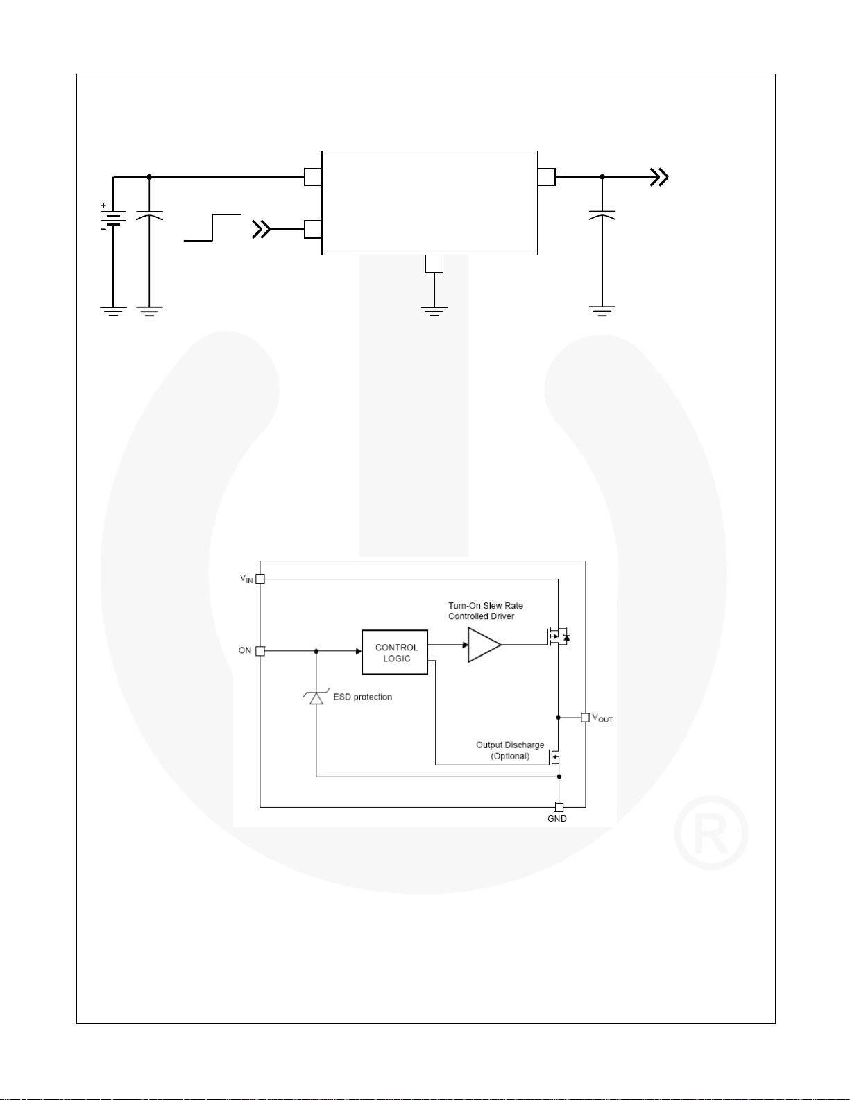
Figure 1. Typical Application
V
OUT
C
OUT
To Load
FPF1107/8
Figure 2. Block Diagram (Output Discharge for FPF1108 Only)
© 2009 Fairchild Semiconductor Corporation www.fairchildsemi.com
FPF1107 / FPF1108 • Rev. 1.0.1 2
A2A
A
Pin Configurations
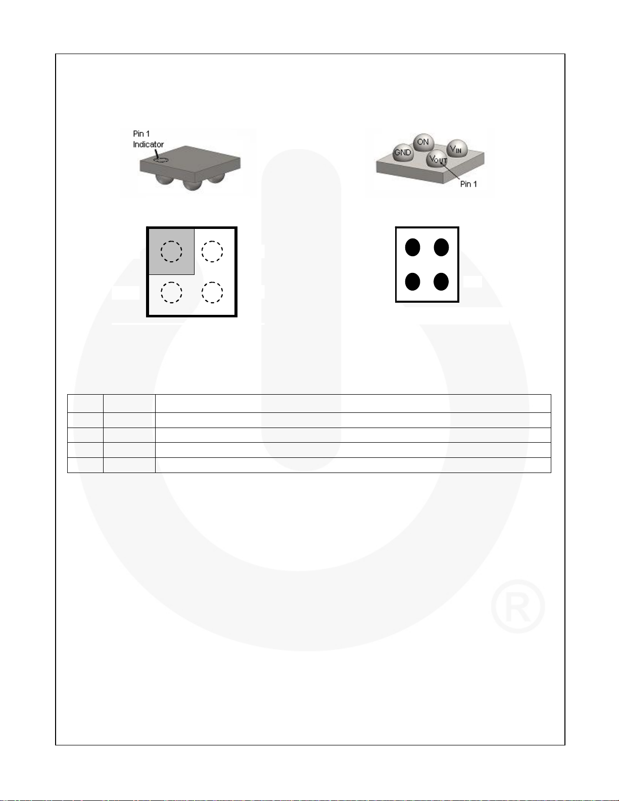
Figure 3. 1 x 1mm WLCSP Bumps Facing Down Figure 4. 1 x 1mm WLCSP Bumps Facing Up
1
V
V
OUT
A1 A2
V
IN
IN
V
OUT
FPF1107 / FPF1108 — Advance Load Management Switch
GND
Figure 5. Pin Assignments (Top View) Figure 6. Pin
B1 B2
ON
Pin Definitions
Pin # Name Description
A1 V
A2 VIN Supply Input: Input to the Power Switch.
B1 GND Ground
B2 ON ON/OFF Control, Active HIGH
Switch Output
OUT
ON
B2 B1
ssignments (Bottom View)
GND
© 2009 Fairchild Semiconductor Corporation www.fairchildsemi.com
FPF1107 / FPF1108 • Rev. 1.0.1 3
FPF1107 / FPF1108 — Advance Load Management Switch
Absolute Maximum Ratings
Stresses exceeding the absolute maximum ratings may damage the device. The device may not function or be
operable above the recommended operating conditions and stressing the parts to these levels is not recommended.
In addition, extended exposure to stresses above the recommended operating conditions may affect device reliability.
The absolute maximum ratings are stress ratings only.
Symbol Parameter Min. Max. Unit
VIN VIN, V
ISW Maximum Continuous Switch Current 1.2 A
PD Power Dissipation at TA=25°C 1.0 W
T
Storage Junction Temperature -65 +150 °C
STG
TA Operating Temperature Range -40 +85 °C
ΘJA
ESD Electrostatic Discharge Capability
Thermal Resistance, Junction-to-Ambient
, VON to GND -0.3 4.2 V
OUT
1S2P with 1 Thermal Via 95
1S2P without Thermal Via 187
Human Body Model,
JESD22-A114
Charged Device Model,
JESD22-C101
4
2
°C/W
kV
Recommended Operating Conditions
The Recommended Operating Conditions table defines the conditions for actual device operation. Recommended
operating conditions are specified to ensure optimal performance to the datasheet specifications. Fairchild does not
recommend exceeding them or designing to Absolute Maximum Ratings.
Symbol Parameter Min. Max. Unit
VIN Supply Voltage 1.2 4.0 V
TA Ambient Operating Temperature -40 +85 °C
© 2009 Fairchild Semiconductor Corporation www.fairchildsemi.com
FPF1107 / FPF1108 • Rev. 1.0.1 4
FPF1107 / FPF1108 — Advance Load Management Switch
Electrical Characteristics
Unless otherwise noted, VIN=1.2 to 4.0V, TA=-40 to +85°C, typical values are at VIN=3.3V and TA=25°C.
Symbol Parameter Conditions Min. Typ. Max. Units
Basic Operation
VIN Supply Voltage 1.2 4.0 V
I
Off Supply Current VON=GND V
Q(OFF)
I
Off Switch Current VON=GND V
SD(OFF)
I
=0mA, VON=VIN 1
IQ Quiescent Current
OUT
I
=0mA, VON < VIN 3
OUT
=3.3V, I
V
IN
VIN=1.8V, I
RON On Resistance
VIN=1.5V, I
VIN=1.2V, I
VIN=1.8V, I
=3.3V, VON=0V, I
V
RPD Output Discharge R
PULL DOWN
IN
T
=25°C, FPF1108
A
VIH On Input Logic High Voltage VIN=1.2V to 4.0V 1.1 V
VIL On Input Logic Low Voltage VIN=1.2V to 4.0V 0.35 V
ION On Input Leakage VON=VIN or GND -1 1 μA
Dynamic Characteristics
t
Turn-On Delay
DON
tR V
t
ON
t
Turn-On Delay
DON
tR V
t
ON
Rise Time
OUT
Turn-On Time
Rise Time
OUT
Turn-On Time
(4)
(4,6)
(4)
(4,6)
(4)
VIN=3.3V, RL=10Ω, CL=0.1µF,
=25°C, FPF1107/8
T
A
(4)
VIN=3.3V, RL=500Ω, CL=0.1µF,
=25°C, FPF1107/8
T
A
FPF1107
t
Turn-Off Delay
DOFF
tF V
t
Turn-Off
OFF
t
Turn-Off Delay
DOFF
tF V
t
Turn-Off
OFF
FPF1108
t
Turn-Off Delay
DOFF
tF V
t
Turn-Off
OFF
t
Turn-Off Delay
DOFF
tF V
t
Turn-Off
OFF
Fall Time
OUT
Fall Time
OUT
(5)
Fall Time
OUT
Fall Time
OUT
(4)
(4)
2.2 μs
(4,7)
4.2 μs
(4)
(4)
110 μs
(4,7)
117 μs
(4)
(4)
1.9 μs
(4,7)
3.9 μs
(4)
(4)
10.6 μs
(4,7)
13.1 μs
=3.3V, RL=10Ω, CL=0.1µF,
V
IN
=25°C
T
A
=3.3V, RL=500Ω, CL=0.1µF,
V
IN
=25°C
T
A
=3.3V, RL=10Ω, CL=0.1µF,
V
IN
R
=65Ω, TA=25°C
PD
VIN=3.3V, RL=500Ω, CL=0.1µF,
=65Ω, TA=25°C
R
PD
Notes:
3. This parameter is guaranteed by design and characterization; not production tested.
4. t
DON/tDOFF/tR/tF
are defined in Figure 7.
5. Output discharge path is enabled during off.
=Open, VIN=4V 1 μA
OUT
=GND 1 μA
OUT
=200mA, TA=25°C 35 50
OUT
=200mA, TA=25°C 55 70
OUT
=200mA, TA=25°C 70
OUT
=200mA, TA=25°C 85 150
OUT
=200mA, TA=85°C
OUT
FORCE
=20mA,
(3)
65 100
65 110 Ω
80 μs
130 μs
210 μs
70 95 μs
95 120 μs
165 215 μs
2.0 2.5 μs
7.0 μs
2.0 2.5 μs
2.5 μs
μA
mΩ
© 2009 Fairchild Semiconductor Corporation www.fairchildsemi.com
FPF1107 / FPF1108 • Rev. 1.0.1 5
 Loading...