FODM3062, FODM3063, FODM3082, FODM3083 — 4-Pin Full Pitch Mini-Flat Package Zero-Cross Triac Driver Output Optocouplers
September 2010
FODM3062, FODM3063, FODM3082, FODM3083
4-Pin Full Pitch Mini-Flat Package Zero-Cross
Triac Driver Output Optocouplers
Features
■
dv/dt of 600V/µs guaranteed
Compact 4-pin surface mount package
■
(2.4mm maximum standoff height)
■
Zero voltage crossing
Peak blocking voltage: 600V (FODM306X)
■
800V (FODM308X)
Available in tape and reel quantities of 2500
■
■
C-UL, UL and VDE certifications pending
Applications
■
Solenoid/valve controls
Lighting controls
■
■
Static power switches
AC motor drives
■
■
Temperature controls
■
E.M. contactors
AC motor starters
■
■
Solid state relays
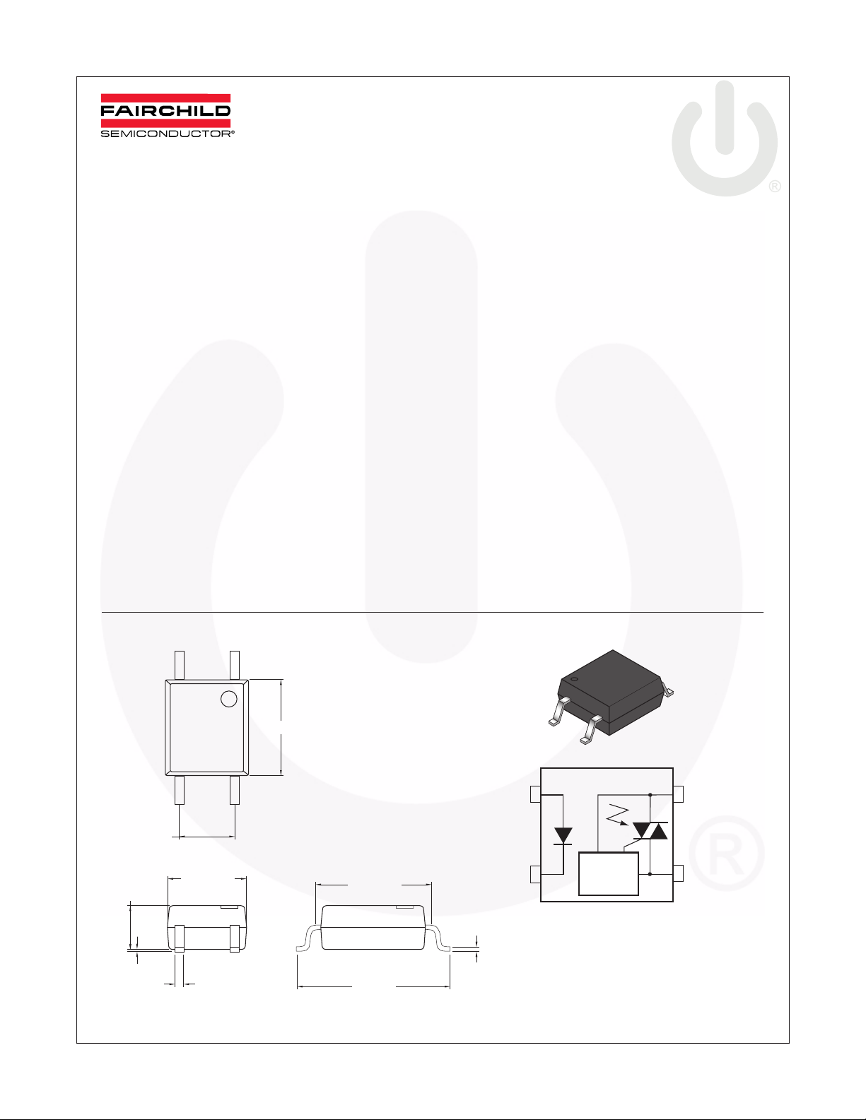
Package Dimensions
Description
The FODM306X and FODM308X series consist of an
infrared emitting diode optically coupled to a monolithic
silicon detector performing the function of a zero voltage
crossing bilateral triac driver, and is housed in a compact
4-pin mini-flat package. The lead pitch is 2.54mm. They
are designed for use with a triac in the interface of logic
systems to equipment powered from 115/240 VAC lines,
such as solid state relays, industrial controls, motors,
solenoids and consumer appliances.
4.40±0.20
ANODE
1
2.54±0.25
ZERO
3.60±0.30
2.00±0.20
0.10±0.10
0.40±0.10
Note:
All dimensions are in millimeters.
©2006 Fairchild Semiconductor Corporation www.fairchildsemi.com
FODM3062, FODM3063, FODM3082, FODM3083 Rev. 1.0.9
5.30±0.30
+0.2
7.00
–0.7
CATHODE
0.20±0.05
2
CROSSING
CIRCUIT
MAIN TERM.
4
3
MAIN TERM.

(T
Absolute Maximum Ratings
= 25°C unless otherwise specified)
A
Stresses exceeding the absolute maximum ratings may damage the device. The device may not function or be
operable above the recommended operating conditions and stressing the parts to these levels is not recommended.
In addition, extended exposure to stresses above the recommended operating conditions may affect device reliability.
The absolute maximum ratings are stress ratings only.
Symbol Parameter Rating Units
TOTAL PACKAGE
T
STG
T
OPR
EMITTER
I
F (avg)
I
F (pk)
V
R
P
D
DETECTOR
I
T(RMS)
V
DRM
P
D
Storage Temperature -55 to +150 °C
Operating Temperature -40 to +100 °C
Continuous Forward Current 60 mA
Peak Forward Current (1µs pulse, 300pps.) 1 A
Reverse Input Voltage 6 V
Power Dissipation (No derating required over operating temp. range) 100 mW
On-State RMS Current 70 mA (RMS)
Off-State Output Terminal Voltage FODM3062/FODM3063 600 V
FODM3082/FODM3083 800
Power Dissipation (No derating required over operating temp. range) 300 mW
FODM3062, FODM3063, FODM3082, FODM3083 — 4-Pin Full Pitch Mini-Flat Package Zero-Cross Triac Driver Output Optocouplers
©2006 Fairchild Semiconductor Corporation www.fairchildsemi.com
FODM3062, FODM3063, FODM3082, FODM3083 Rev. 1.0.9 2

(T
Electrical Characteristics
= 25°C)
A
Individual Component Characteristics
Symbol Parameter Test Conditions Min. Typ.* Max. Units
EMITTER
V
Input Forward Voltage I
F
I
Reverse Leakage Current V
R
= 30mA 1.5 V
F
= 6V 100 µA
R
DETECTOR
I
DRM1
Peak Blocking Current,
Either Direction
dV/dt Critical Rate of Rise of
Off-State Voltage
Rated V
I
DRM
= 0 (Figure 1)
F
(1)
, I
= 0
F
(2)
600 V/µs
500 nA
Transfer Characteristics
Symbol DC Characteristics Test Conditions Device Min. Typ.* Max. Units
I
V
I
LED Trigger Current Main Terminal
FT
Holding Current,
H
Either Direction
Peak On-State Voltage,
TM
Either Direction
Voltage = 3V
I
= Rated I
F
I
= 100mA peak
TM
FT
(3)
FODM3062 10 mA
FODM3082
FODM3063 5
FODM3083
All 300 µA
,
All 3 V
FODM3062, FODM3063, FODM3082, FODM3083 — 4-Pin Full Pitch Mini-Flat Package Zero-Cross Triac Driver Output Optocouplers
Zero Crossing Characteristics
Symbol Characteristics Test Conditions Device Min. Typ.* Max. Units
V
IH
Inhibit Voltage,
MT1-MT2 Voltage
above which device
will not trigger
IDRM2 Leakage in Inhibit
State
I
= Rated I
F
I
= Rated I
F
FT
Rated VDRM,
Off-State
All 20 V
FT
,
All 2 mA
Isolation Characteristics
Characteristics Test Conditions Symbol Device Min. Typ.* Max. Units
Steady State Isolation
(4)
Voltage
*All typicals at 25°C.
Notes:
1. Test voltage must be applied within dv/dt rating.
2. This is static dv/dt. See Figure 1 for test circuit. Commutating dv/dt is function of the load-driving thyristor(s) only.
3. All devices are guaranteed to trigger at an I
I
lies between max I
F
4. Steady state isolation voltage, V
common, and pins 3 & 4 are common.
(1 Minute)
V
ISO
All 3750 VRMS
R.H. = 40% to 60%
value less than or equal to max I
(10mA for FODM3062/82, 5mA for FODM3063/83) and absolute max I
FT
ISO
F
, is an internal device dielectric breakdown rating. For this test, pins 1 & 2 are
. Therefore, recommended operating
FT
(60 mA).
F
©2006 Fairchild Semiconductor Corporation www.fairchildsemi.com
FODM3062, FODM3063, FODM3082, FODM3083 Rev. 1.0.9 3

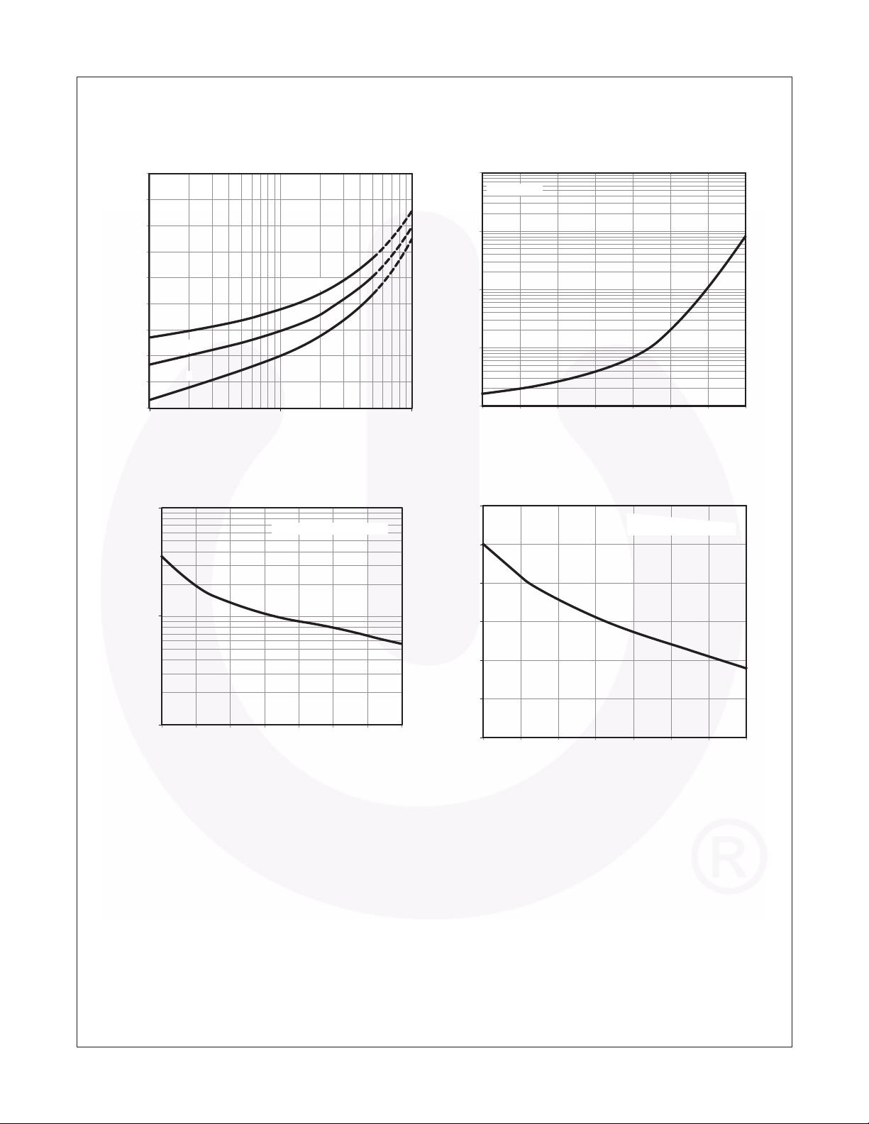
Typical Performance Curves
Fig. 1 LED Forward Voltage vs. Forward Current Fig. 2 Leakage Current vs. Ambient Temperature
1.8
1.7
1000
VDRM = 600V
FODM3062, FODM3063, FODM3082, FODM3083 — 4-Pin Full Pitch Mini-Flat Package Zero-Cross Triac Driver Output Optocouplers
1.6
1.5
1.4
1.3
1.2
- FORWARD VOLTAGE (V)
F
V
TA = 25°C
1.1
TA = 100°C
1.0
0.9
110100
IF - FORWARD CURRENT (mA)
TA = -40°C
Fig. 3 Holding Current vs. Ambient Temperature Fig. 4 Trigger Current vs. Ambient Temperature
10
NORMALIZED TO TA = 25°C
1.0
100
10
- LEAKAGE CURRENT (nA)
1
DRM
I
0.1
-40 -20 0 20 406080100
TA - AMBIENT TEMPERATURE (°C)
1.6
1.4
1.2
1.0
= 3V
V
TM
NORMALIZED TO T
= 25°C
A
0.8
- HOLDING CURRENT (NORMALIZED)
H
I
0.1
-40 -20 100
020406080
TA - AMBIENT TEMPERATURE (°C)
- TRIGGER CURRENT (NORMALIZED)
0.6
FT
I
0.8
-40 -20 0 20 40 60 80
TA - AMBIENT TEMPERATURE (°C)
100
©2006 Fairchild Semiconductor Corporation www.fairchildsemi.com
FODM3062, FODM3063, FODM3082, FODM3083 Rev. 1.0.9 4
 Loading...