Fairchild FOD420 service manual

FOD420, FOD4208, FOD4216, FOD4218 — 6-Pin DIP Triac Drivers
July 2009
FOD420, FOD4208, FOD4216, FOD4218
6-Pin DIP Triac Drivers
Features
■
300mA on-state current
High blocking voltage
■
– 800V (FOD4208, FOD4218)
– 600V (FOD420, FOD4216)
■
High trigger sensitivity
– 1.3mA (FOD4216, FOD4218)
– 2mA (FOD420, FOD4208)
■
High static dv/dt (10,000V/µs)
6 pin DIP dual in-line package
■
– available with surface mount leadform.
Lead free assembly
■
■
UL, VDE, FIMKO and C-UL approved
Description
The FOD420, FOD4208, FOD4216 and FOD4218
devices consist of an infrared emitting diode coupled to a
hybrid random phase triac formed with two inverse
parallel SCRs which form the triac function capable of
driving discrete triacs. The FOD4216 and FOD4218
utilize a high efficiency infrared emitting diode which
offers an improved trigger sensitivity. These devices are
housed in a standard 6-pin dual in-line (DIP) package.
Applications
■
Solid-state relays
Industrial controls
■
■
Lighting controls
Static power switches
■
■
AC motor starters
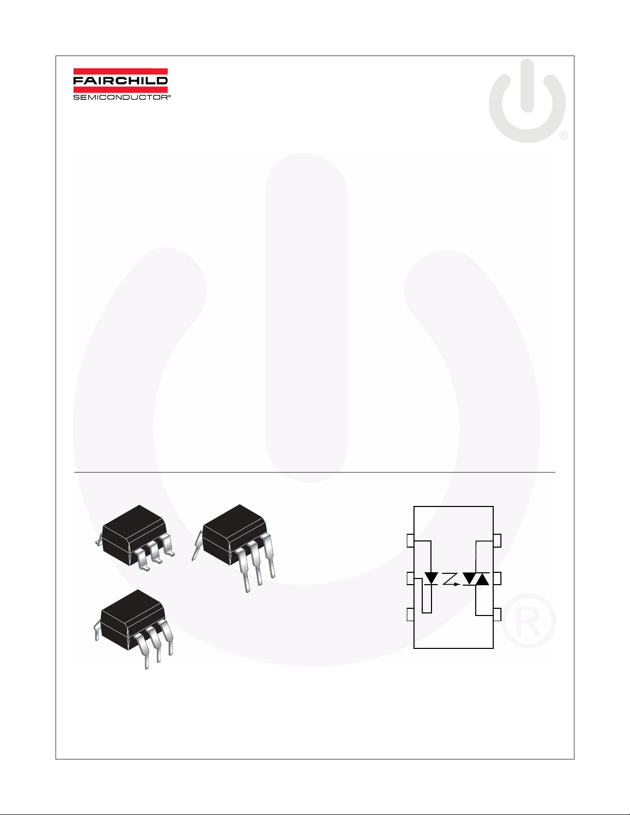
PackageSchematic
ANODE
6
1
6
CATHODE
1
2
MAIN TERM.
6
NC*
5
1
3
N/C
6
*DO NOT CONNECT
(TRIAC SUBSTRATE)
4
MAIN TERM.
1
©2004 Fairchild Semiconductor Corporation www.fairchildsemi.com
FOD420, FOD4208, FOD4216, FOD4218 Rev. 1.4.0

FOD420, FOD4208, FOD4216, FOD4218 — 6-Pin DIP Triac Drivers
Absolute Maximum Ratings
(T
= 25°C unless otherwise noted)
A
Stresses exceeding the absolute maximum ratings may damage the device. The device may not function or be
operable above the recommended operating conditions and stressing the parts to these levels is not recommended.
In addition, extended exposure to stresses above the recommended operating conditions may affect device reliability.
The absolute maximum ratings are stress ratings only.
Symbol Parameters Device Value Units
TOTAL DEVICE
T
STG
T
OPR
T
SOL
T
V
P
DTOTAL
EMITTER
V
P
DETECTOR
V
DRM
I
TSM
I
P
DDET
Note:
1. Isolation voltage, V
and Pins 4, 5 and 6 are common. 5,000 VRMS for 1 minute duration is equivalent to 6,000 VRMS for 1 second
duration.
Storage Temperature All -55 to +150 °C
Operating Temperature All -55 to +100 °C
Lead Solder Temperature (Wave) All 260 for 10 sec °C
Junction Temperature Range All 125 °C
J
Isolation Test Voltage
ISO
(1)
All 5000 Vac(rms)
(rms AC voltage, 60Hz, 1 min. duration)
Total Device Power Dissipation @ 25°C
Derate above 40°C
Continuous Forward Current All 30 mA
I
F
Reverse Voltage All 6 V
R
Total Power Dissipation 25°C Ambient
DE
Derate above 40°C
All 500 mW
6.6 mW/°C
All 50 mW
0.71 mW/°C
Off-State Output Terminal Voltage FOD420, FOD4216 600 V
FOD4208, FOD4218 800
Peak Non-Repetitive Surge Current
All 3 A
(single cycle 60Hz sine wave)
Peak On-State Current All 300 mA
TM
Total Power Dissipation @ 25°C Ambient
Derate above 40°C
, is an internal device dielectric breakdown rating. For this test, Pins 1, 2 and 3 are common,
ISO
All 450 mW
5.9 mW/°C
©2004 Fairchild Semiconductor Corporation www.fairchildsemi.com
FOD420, FOD4208, FOD4216, FOD4218 Rev. 1.4.0 2

≤
FOD420, FOD4208, FOD4216, FOD4218 — 6-Pin DIP Triac Drivers
Electrical Characteristics
(T
= 25°C Unless otherwise specified)
A
Individual Component Characteristics
Symbol Parameters Test Conditions Device Min. Typ.* Max Units
EMITTER
Input Forward Voltage I
V
F
Reverse Leakage
I
R
= 20mA All 1.28 1.5 V
F
V
= 6V All 0.01 10 µA
R
Current
DETECTOR
I
DRM
Peak Blocking Current,
Either Direction
I
= 0,
F
= 100°C
T
A
(2)
V
= 800V FOD4208,
D
FOD4218
= 600V FOD420,
V
D
3 100 µA
FOD4216
I
R(RMS)
Reverse Current T
= 100°C V
A
= 800V FOD4208,
D
3 100 µA
FOD4218
= 600V FOD420,
V
D
FOD4216
(4)
= 0
dv/dt Critical Rate of Rise of
(Fig. 11) 10,000 V/µs
I
F
Off-State Voltage
Transfer Characteristics
Symbol DC Characteristics Test Conditions Device Min. Typ.* Max. Units
I
LED Trigger Current Main Terminal Voltage = 5V
FT
V
Peak On-State Voltage,
TM
Either Direction
Holding Current,
I
H
Either Direction
Latching Current V
I
L
t
t
dv/dt
Tu r n-On Time PF = 1.0,
ON
Tu r n-Off Time V
OFF
Critical Rate of Rise of
crq
Voltage at Current
Commutation
di/dt
Critical Rate of Rise of
cr
On-State Current
dV(IO)/dt Critical Rate of Rise of
Coupled Input/Output
Voltage
I
= 300 mA peak, I
TM
V
= 3V All 200 500 µA
T
= 2.2V All 5 mA
T
V
= 300mA
I
T
V
V
V
= 0.67 V
D
di/dt
= 0A,
I
T
V
RM
crq
= V
15 A/ms
DM
T
,
DRM
T
= 424VAC
(3)
FOD420,
0.75 2.0 mA
FOD4208
FOD4216,
0.75 1.3
FOD4218
= rated I
F
= V
RM
= V
RM
FT
= 565 VAC FOD4208 60 µs
DM
= 424 VAC FOD420,
DM
All 2.2 3 V
FOD4216,
FOD4218
= V
RM
RM
= 565 VAC FOD4208 52 µs
DM
= V
= 424 VAC FOD420,
DM
FOD4216,
FOD4218
= 25°C All 10,000 V/µs
j
= 80°C 5,000
j
All 8 A/µs
All
10,000
V/µs
Isolation Characteristics
Symbol Characteristics Test Conditions Min. Typ.* Max. Units
V
ISO
Input-Output Isolation
f = 60Hz, t = 1 min.
Voltage
*Typical values at T
©2004 Fairchild Semiconductor Corporation www.fairchildsemi.com
FOD420, FOD4208, FOD4216, FOD4218 Rev. 1.4.0 3
= 25°C
A
(5)
5000 Vac(rms)

Notes:
2. Test voltage must be applied within dv/dt rating.
3. All devices are guaranteed to trigger at an I
I
lies between max I
F
max I
(30mA).
F
(2mA for FOD420 and FOD4208 and 1.3mA for FOD4216 and FOD4218 and the absolute
FT
value less than or equal to max I
F
. Therefore, recommended operating
FT
4. This is static dv/dt. See Figure 11 for test circuit. Commutating dv/dt is a function of the load-driving thyristor(s) only.
5. Isolation voltage, V
, is an internal device dielectric breakdown rating. For this test, Pins 1, 2 and 3 are common,
ISO
and Pins 4, 5 and 6 are common.
Typical Application
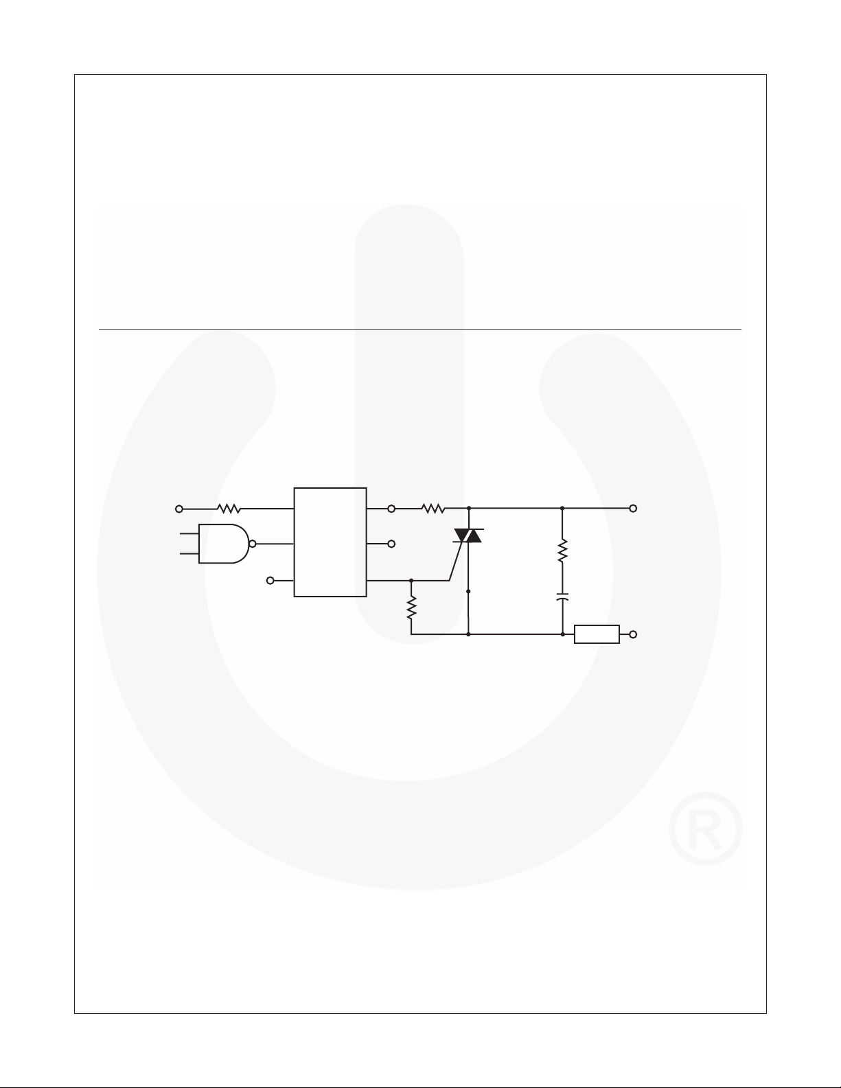
Typical circuit for use when hot line switching is required.
In this circuit the “hot” side of the line is switched and the
load connected to the cold or neutral side. The load may
be connected to either the neutral or hot line.
R
is calculated so that I
in
is equal to the rated I
F
FT
of the
part, 2mA for FOD420 and FOD4208, 1.3mA for
FOD4216 and FOD4218. The 39Ω resistor and 0.01µF
capacitor are for snubbing of the triac and may or may
not be necessary depending upon the particular triac
and load use.
FOD420, FOD4208, FOD4216, FOD4218 — 6-Pin DIP Triac Drivers
R
in
V
CC
* For highly inductive loads (power factor < 0.5), change this value to 360 ohms
1
2
3
FOD420
FOD4208
FOD4216
FOD4218
330
360 Ω
6
5
4
Ω
FKPF12N80
39*Ω
0.01µF
LOAD
.
HOT
240 VAC
NEUTRAL
Figure 1. Hot-Line Switching Application Circuit
©2004 Fairchild Semiconductor Corporation www.fairchildsemi.com
FOD420, FOD4208, FOD4216, FOD4218 Rev. 1.4.0 4
 Loading...