Fairchild FOD3180 service manual

FOD3180 — 2A Output Current, High Speed MOSFET Gate Driver Optocoupler
August 2008
FOD3180
2A Output Current, High Speed MOSFET Gate Driver
Optocoupler
Features
Guaranteed operating temperature range of -40°C to
■
+100°C
■
2A minimum peak output current
■
High speed response: 200ns max propagation delay
over temperature range
■
250kHz maximum switching speed
■
30ns typ pulse width distortion
Wide V
■
■
5000Vrms, 1 minute isolation
■
Under voltage lockout protection (UVLO) with
operating range: 10V to 20V
CC
hysteresis
Minimum creepage distance of 7.0mm
■
■
Minimum clearance distance of 7.0mm
C-UL, UL and VDE* approved
■
R
■
■
15kV/µs minimum common mode rejection
of 1.5 Ω (typ.) offers lower power dissipation
DS(ON)
Applications
■
Plasma Display Panel
High performance DC/DC convertor
■
■
High performance switch mode power supply
■
High performance uninterruptible power supply
Isolated Power MOSFET gate drive
■
*Requires ‘V’ ordering option
Description
The FOD3180 is a 2A Output Current, High Speed
MOSFET Gate Drive Optocoupler. It consists of a
aluminium gallium arsenide (AlGaAs) light emitting diode
optically coupled to a CMOS detector with PMOS and
NMOS output power transistors integrated circuit power
stage. It is ideally suited for high frequency driving of
power MOSFETs used in Plasma Display Panels
(PDPs), motor control inverter applications and high
performance DC/DC converters.
The device is packaged in an 8-pin dual in-line housing
compatible with 260°C reflow processes for lead free
solder compliance.
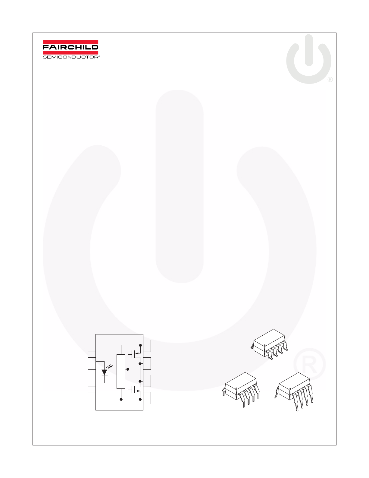
Functional Block Diagram Package Outlines
FOD3180
NO CONNECTION
ANODE
CATHODE
NO CONNECTION
Note:
A 0.1µF bypass capacitor must be connected between pins 5 and 8.
©2005 Fairchild Semiconductor Corporation www.fairchildsemi.com
FOD3180 Rev. 1.0.6
1
2
3
4
8
VCC
7
OUTPUT
OUTPUT
6
5
VEE
8
1
8
1
8
1

FOD3180 — 2A Output Current, High Speed MOSFET Gate Driver Optocoupler
Absolute Maximum Ratings
(T
= 25°C unless otherwise specified)
A
Stresses exceeding the absolute maximum ratings may damage the device. The device may not function or be
operable above the recommended operating conditions and stressing the parts to these levels is not recommended.
In addition, extended exposure to stresses above the recommended operating conditions may affect device reliability.
The absolute maximum ratings are stress ratings only.
Symbol
T
STG
T
OPR
T
J
T
SOL
I
F(AVG)
I
F(tr, tf)
I
F(TRAN)
V
R
I
OH(PEAK)
I
OL(PEAK)
V
– V
CC
V
O(PEAK)
P
O
P
D
EE
Parameter
Value Units
Storage Temperature -40 to +125 °C
Operating Temperature -40 to +100 °C
Junction Temperature -40 to +125 °C
Lead Solder Temperature 260 for 10 sec. °C
Average Input Current
(1)
25 mA
LED Current Minimum Rate of Rise/Fall 250 ns
Peak Transient Input Current (<1µs pulse width, 300pps) 1.0 A
Reverse Input Voltage 5 V
“High” Peak Output Current
“Low” Peak Output Current
(2)
2.5 A
(2)
2.5 A
Supply Voltage -0.5 to 25 V
Output Voltage 0 to V
Output Power Dissipation
Total Power Dissipation
(4)
250 mW
(5)
295 mW
CC
V
Recommended Operating Conditions
The Recommended Operating Conditions table defines the conditions for actual device operation. Recommended
operating conditions are specified to ensure optimal performance to the datasheet specifications. Fairchild does not
recommend exceeding them or designing to absolute maximum ratings.
Symbol
V
– V
CC
I
F(ON)
V
F(OFF)
EE
Parameter
Power Supply 10 to 20 V
Input Current (ON) 10 to 16 mA
Input Voltage (OFF) -3.0 to 0.8 V
Value Units
©2005 Fairchild Semiconductor Corporation www.fairchildsemi.com
FOD3180 Rev. 1.0.6 2

∆
Electrical-Optical Characteristics (DC)
Over recommended operating conditions unless otherwise specified.
Symbol Parameter Test Conditions Min. Typ.* Max. Unit
I
OH
I
OL
V
V
I
CCH
I
CCL
I
FLH
OH
OL
High Level Output Current
Low Level Output Current
High Level Output Voltage
Low Level Output Voltage
High Level Supply Current Output Open,
Low Level Supply Current Output Open,
Threshold Input Current Low to
High
V
FHL
V
V
F
Threshold Input Voltage High to Low I
Input Forward Voltage I
F
/T
Temperature Coefficient of Forward
A
Voltage
V
UVLO+
V
UVLO–
UVLO
BV
C
IN
UVLO Threshold V
UVLO Hysteresis 0.6 V
HYST
Input Reverse Breakdown Voltage I
R
Input Capacitance f = 1MHz, V
*Typical values at T
= 25°C
A
(2)(3)
(2)(3)
(6)(7)
(6)(7)
I
V
= (V
– V
OH
V
OH
V
OL
V
OL
I
O
O
CC
= (V
CC
= (V
CC
= (V
CC
= -100mA V
= 100mA V
– 1V) 0.5 A
EE
– V
– 3V) 2.0
EE
– V
– 1V) 0.5 A
EE
– V
– 3V) 2.0
EE
– 0.5 V
CC
+ 0.5 V
EE
4.8 6.0 mA
I
= 10 to 16mA
F
5.0 6.0 mA
V
= -3.0 to 0.8V
F
I
= 0mA, V
O
= 0mA, V
O
= 10mA 1.2 1.43 1.8 V
F
I
= 10mA -1.5 mV/°C
F
> 5V, I
O
V
< 5V, I
O
= 10µA 5 V
R
> 5V 8.0 mA
O
< 5V 0.8 V
O
= 10mA 8.3 V
F
= 10mA 7.7 V
F
= 0V 60 pF
F
FOD3180 — 2A Output Current, High Speed MOSFET Gate Driver Optocoupler
©2005 Fairchild Semiconductor Corporation www.fairchildsemi.com
FOD3180 Rev. 1.0.6 3

FOD3180 — 2A Output Current, High Speed MOSFET Gate Driver Optocoupler
Switching Characteristics
Over recommended operating conditions unless otherwise specified.
Symbol
t
t
P
P
DD
(t
PHL
t
UVLO ON
t
UVLO OFF
| CM
PLH
PHL
WD
– t
t
r
t
f
Parameter
Propagation Delay Time to High Output Level
Propagation Delay Time to Low Output Level
Pulse Width Distortion
Propagation Delay Difference Between Any
)
Two Pa rts
PLH
(10)
(9)
Test Conditions Min. Typ.* Max. Unit
(8)
I
F
R
(8)
50 105 200 ns
f = 250kHz,
Duty Cycle = 50%,
C
Rise Time CL = 10nF,
Fall Time 55 ns
R
UVLO Turn On Delay 2.0 µs
UVLO Turn Off Delay 0.3 µs
| Output High Level Common Mode Transient
H
Immunity
(11) (12)
TA = +25°C,
I
f
V
V
| CM
| Output Low Level Common Mode Transient
L
Immunity
(11) (13)
TA = +25°C,
V
V
V
*Typical values at T
= 25°C
A
= 10mA,
= 10 Ω ,
g
= 10nF
g
= 10Ω
g
= 10 to 16mA,
= 1.5kV,
CM
= 20V
CC
= 0V,
f
= 1.5kV,
CM
= 20V
CC
50 135 200 ns
65 ns
-90 90 ns
75 ns
15 kV/µs
15 kV/µs
Isolation Characteristics
Symbol
V
R
C
*Typical values at T
Parameter
Withstand Isolation Voltage
ISO
Resistance (input to output)
I-O
Capacitance (input to output) Freq. = 1MHz 1 pF
I-O
= 25°C
A
(14) (15)
(15)
Test Conditions Min. Typ.* Max. Unit
TA = 25°C,
R.H. < 50%, t = 1min.,
I
≤ 20µA
I-O
V
= 500V 10
I-O
5000 V
11
rms
Ω
©2005 Fairchild Semiconductor Corporation www.fairchildsemi.com
FOD3180 Rev. 1.0.6 4
 Loading...