FOD0721, FOD0720, FOD0710 — High CMR, 25Mbit/sec Logic Gate Optocoupler
December 2010
FOD0721, FOD0720, FOD0710
High CMR, 25Mbit/sec Logic Gate Optocoupler
Features
■
20kV/µs minimum CMR
40ns max. propagation delay
■
■
Data Rate, Non-Return Zero Coding
– 25Mbit/sec (FOD0721 and FOD0720)
– 12.5Mbit/sec (FOD0710)
■
Pulse Width Distortion
– 6ns (FOD0721)
– 8ns (FOD0720 and FOD0710)
■
+5V CMOS compatibility
Extended industrial temperate range
■
– -40 to 100°C temperature range
Safety and regulatory approvals
■
– UL1577, 3750 VACrms for 1 min. (File #E90700,
Volume 2)
– IEC60747-5-2 pending approval
Applications
Industrial fieldbus communications
■
– Profibus, DeviceNet, CAN, RS485
Programmable logic control
■
■
Isolated data acquisition system
Description
The FOD0721/0720/0710 family utilizes Fairchild’s
proprietary coplanar packaging technology, Optoplanar,
and optimized IC design to guarantee minimum 20kV/µs
Common Mode Noise Rejection (CMR) rating.
These high-speed logic gate optocouplers consist of a
high-speed AlGaAs LED driven by a CMOS IC coupled
to a CMOS detector IC, comprising an integrated photodiode, a high-speed transimpedance amplifier and a
voltage comparator with an output driver. The CMOS
technology coupled to the high efficiency of the LED
achieves low power consumption as well as very high
speed (40ns propagation delay, 6ns pulse width
distortion).
These devices are available in a compact 8-pin small
outline package.
®
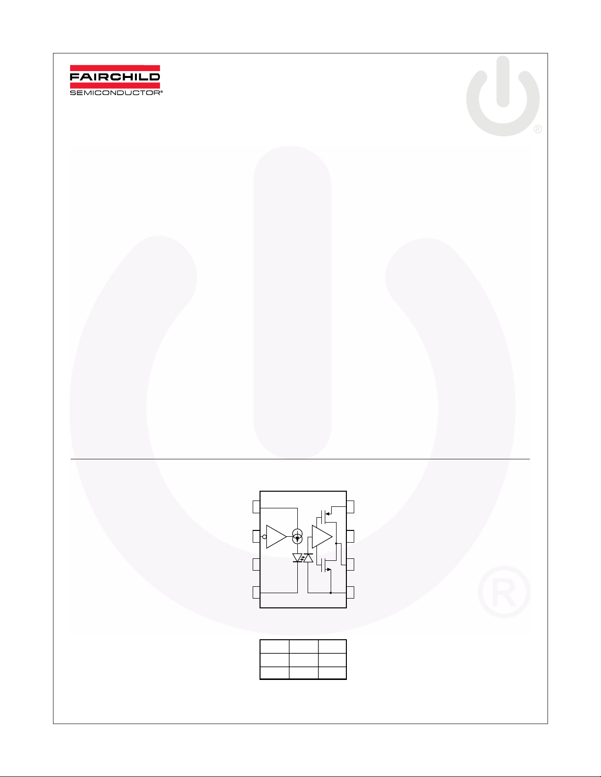
Functional Schematic
V
1
DD1
V
2
I
3
*
GND1
4 5
*: Pin 3 must be left unconnected
Tr uth Table
LED
V
I
H
OFF
L
©2004 Fairchild Semiconductor Corporation www.fairchildsemi.com
FOD0721, FOD0720, FOD0710 Rev. 1.0.9
V
H
ON
V
8
DD2
NC
7
V
6
O
GND2
O
L

Pin Definitions
Pin Number Pin Name Pin Function Description
1V
2V
DD1
I
3 LED Anode – must be left unconnected
4 GND1 Input Ground
5 GND2 Output Ground
6V
O
7NCNot Connected
8V
DD2
Input Supply Voltage
Input Data
Output Data
Output Supply Voltage
FOD0721, FOD0720, FOD0710 — High CMR, 25Mbit/sec Logic Gate Optocoupler
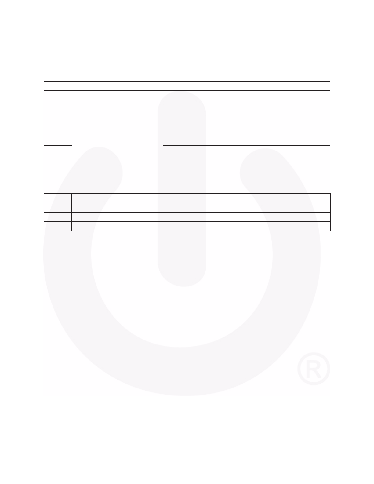
Absolute Maximum Ratings
(T
= 25°C unless otherwise specified.)
A
Stresses exceeding the absolute maximum ratings may damage the device. The device may not function or be
operable above the recommended operating conditions and stressing the parts to these levels is not recommended.
In addition, extended exposure to stresses above the recommended operating conditions may affect device reliability.
The absolute maximum ratings are stress ratings only.
Symbol Parameter Value Units
T
STG
T
OPR
T
SOL
V
DD1
V
I
I
I
V
DD2
V
D
I
O
PD1 Input Power Dissipation 90 mW
PD2 Output Power Dissipation 70 mW
Storage Temperature -40 to +125 °C
Operating Temperature -40 to +100 °C
Lead Solder Temperature 260 for 10 sec °C
Reflow Temperature Profile (Refer to Relow Profile)
Input Supply Voltage 0 to 6.0 V
Input Voltage -0.5 to V
+ 0.5 V
DD1
Input DC Current -10 to +10 mA
Output Supply Voltage 0 to 6.0 V
Output Voltage -0.5 to V
+ 0.5 V
DD2
Average Output Current 10 mA
Recommended Operating Conditions
The Recommended Operating Conditions table defines the conditions for actual device operation. Recommended
operating conditions are specified to ensure optimal performance to the datasheet specifications. Fairchild does not
recommend exceeding them or designing to absolute maximum ratings.
Symbol Parameter Min. Max. Unit
T
OPR
V
, V
DD1
V
IH
V
IL
t
, t
r
f
•A 0.1µF bypass capacitor must be connected between pins 1 and 4, and 5 and 8
• Pin 3 must be left unconnected
©2004 Fairchild Semiconductor Corporation www.fairchildsemi.com
FOD0721, FOD0720, FOD0710 Rev. 1.0.9 2
Ambient Operating Temperature -40 +100 °C
Supply Voltages 4.5 5.5 V
DD2
Logic High Input Voltage 2.0 V
DD1
Logic Low Input Voltage 0 0.8 V
Input Signal Rise and Fall Time 1.0 ms
V

≤
≤
Ω
FOD0721, FOD0720, FOD0710 — High CMR, 25Mbit/sec Logic Gate Optocoupler
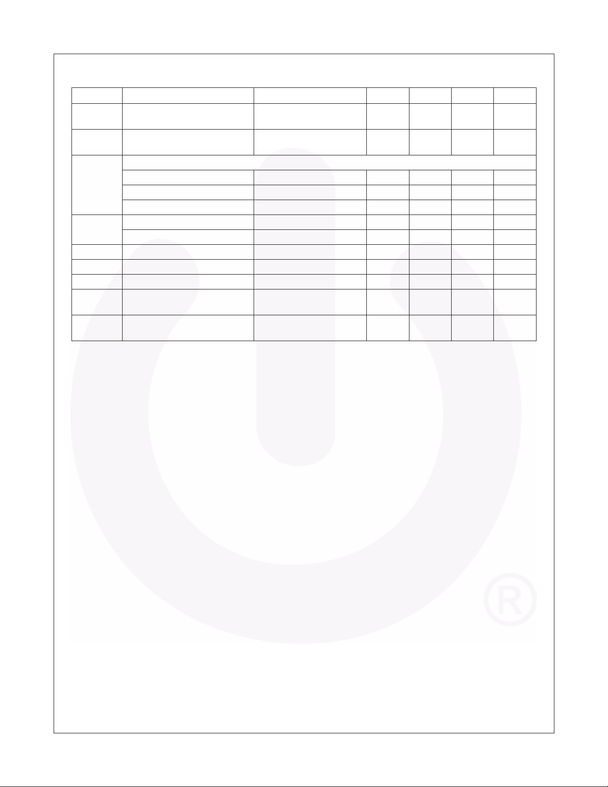
Electrical Characteristics
(T
= -40°C to 100°C and 4.5V ≤ V
A
5.5V, all typicals are at T
DD
= 25°C, V
A
DD
= 5V)
Symbol Parameter Test Conditions Min. Typ. Max. Unit
INPUT CHARACTERISTICS
I
DD1L
I
DD1H
I
DD1
Logic Low Input Supply Current V
Logic High Input Supply Current V
= 0V 6.5 10.0 mA
I
= V
I
DD1
0.8 3.0 mA
Input Supply Current 13.0 mA
I
Input Current -10 +10 µA
I
OUTPUT CHARACTERISTICS
I
DD2L
I
DD2H
V
V
V
V
Isolation Characteristics
Logic Low Output Supply Current V
Logic High Output Supply Current V
Logic High Output Voltage I
OH
OH
Logic Low Output Voltage I
OL
OL
= 0V 5.5 9 mA
I
= V
I
DD1
= -20µA, V
O
I
= -4mA, V
O
= 20µA, V
O
I
= 4mA, V
O
(T
= -40°C to +100°C unless otherwise specified.)
A
= V
I
= V
I
= V
I
= V
I
IH
IH
IL
IL
5.3 9 mA
4.4 5.0 V
4.0 4.8 V
0 0.1 V
0.5 1.0 V
Symbol Characteristics Test Conditions Min. Typ.* Max. Unit
V
R
C
*All typicals at T
Input-Output Isolation Voltage f = 60Hz, t = 1.0 min, I
ISO
Isolation Resistance V
ISO
Isolation Capacitance V
ISO
= 25°C
A
= 500V
I-O
= 0 , f = 1.0MHz
I-O
(1)
I-O
(1)
Notes:
1. Device is considered a two terminal device: Pins 1, 2, 3 and 4 are shorted together and Pins 5, 6, 7 and 8 are shorted
together.
2. 3,750 VAC RMS for 1 minute duration is equivalent to 4,500 VAC RMS for 1 second duration.
10µA
(1)(2)
3750 Vac
11
10
0.2 pF
RMS
©2004 Fairchild Semiconductor Corporation www.fairchildsemi.com
FOD0721, FOD0720, FOD0710 Rev. 1.0.9 3

≤
FOD0721, FOD0720, FOD0710 — High CMR, 25Mbit/sec Logic Gate Optocoupler
Switching Characteristics
(T
= -40°C to 100°C and 4.5V ≤ V
A
5.5V, all typicals are at T
DD
= 25°C, V
A
DD
= 5V)
Symbol Parameter Test Conditions Min. Typ. Max. Unit
t
PHL
t
PLH
PWD Pulse Width Distortion, | t
Data Rate FOD0710
t
PSK
t
R
t
F
|CM
|CM
Notes:
3. t
PSK
temperature within the recommended operating conditions.
4. Common mode transient immunity at output high is the maximum tolerable (positive) dVcm/dt on the leading edge
of the common mode impulse signal. Vcm, to assure that the output will remain high. Common mode transient
immunity at output low is the maximum tolerable (negative dVcm/dt on the trailing edge of the common pulse
signal, Vcm, to assure that the output will remain low.
Propagation Delay Time to
C
= 15pF 21 40 ns
L
Logic Low Output
Propagation Delay Time to
C
= 15pF 23 40 ns
L
Logic High Output
– t
PLH
|
= 15pF 2 8 ns
L
= 15pF 2 8 ns
L
= 15pF 2 6 ns
L
PHL
FOD0710 PW = 80ns, C
FOD0720 PW = 40ns, C
FOD0721 PW = 40ns, C
FOD0720, FOD0721
Propagation Delay Skew C
= 15pF
L
(3)
Output Rise Time (10%–90%) 5 ns
Output Fall Time (90%–10%) 4.5 ns
| Common Mode Transient
H
Immunity at Output High
| Common Mode Transient
L
Immunity at Output Low
is equal to the magnitude of the worst case difference in t
VI = V
VCM = 1000V
VI = 0V, VO < 0.8,
V
CM
, VO > 0.8 V
DD1
= 1000V
(4)
(4)
PHL
DD2
and/or t
20 40 kV/µs
20 40 kV/µs
that will be seen between units at any given
PLH
12.5 Mb/s
25 Mb/s
20 ns
©2004 Fairchild Semiconductor Corporation www.fairchildsemi.com
FOD0721, FOD0720, FOD0710 Rev. 1.0.9 4
 Loading...