FOD060L, FOD260L — 3.3V/5V High Speed-10 MBit/s Logic Gate Optocouplers
October 2011
FOD060L, FOD260L
3.3V/5V High Speed-10 MBit/s
Logic Gate Optocouplers
■
Features
■
FOD060L in SO8 and FOD260L in 8-pin DIP
■
Very high speed – 10 MBit/s
Superior CMR — 50 kV/µs at 1,000V peak
■
■
Fan-out of 8 over -40°C to +85°C
Logic gate output
■
■
Strobable output
Wired OR-open collector
■
■
Safety and regulatory approvals
– UL1577
– DIN EN/IEC 60747-5-2
Applications
■
Ground loop elimination
LSTTL to TTL, LSTTL or 5-volt CMOS
■
Line receiver, data transmission
■
Data multiplexing
Switching power supplies
■
■
Pulse transformer replacement
Computer-peripheral interface
■
Description
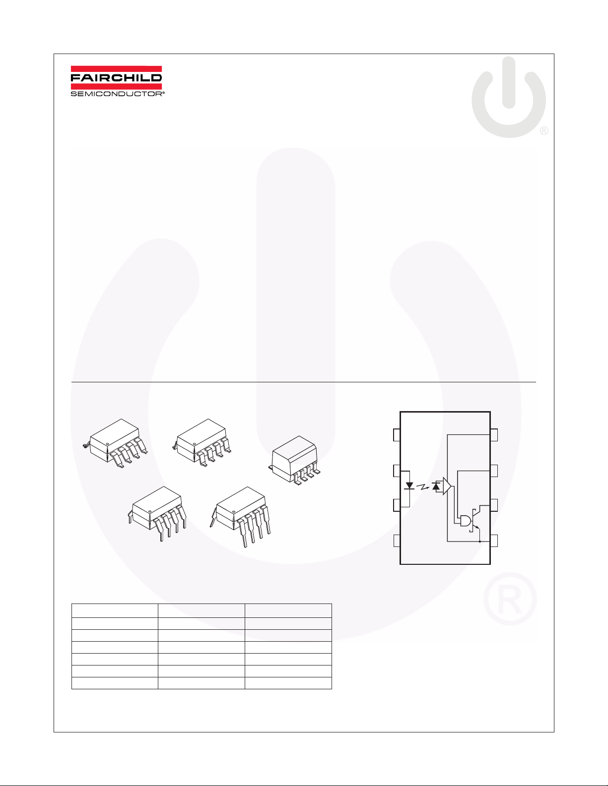
These optocouplers consist of an AlGaAS LED, optically
coupled to a very high speed integrated photo-detector
logic gate. Devices include a strobable output. This
output features an open collector, thereby permitting
wired OR outputs. The coupled parameters are
guaranteed over the temperature range of -40°C to
+85°C. A maximum input signal of 5 mA will provide a
minimum output sink current of 13 mA (fan out of 8). An
internal noise shield provides superior common mode
rejection of typically 50 kV/µs at 1,000V common mode.
Package
8
1
8
8
1
8
1
8
1
1
Truth Table (Positive Logic)
Input Enable Output
On H L
Off H H
On L H
Off L H
On* NC* L*
Off* NC* H*
*Devices with pin 7 not connected.
A 0.1 µF bypass capacitor must be connected between pins 5 and 8. (See Note 1)
N/C
V
N/C
1
+
2
F
_
3
4
8
7
6
5
V
CC
V
E
V
O
GND
©2008 Fairchild Semiconductor Corporation www.fairchildsemi.com
FOD060L, FOD260L Rev. 1.0.5

FOD060L, FOD260L — 3.3V/5V High Speed-10 MBit/s Logic Gate Optocouplers
Absolute Maximum Ratings
(No derating required up to 85°C)
Stresses exceeding the absolute maximum ratings may damage the device. The device may not function or be
operable above the recommended operating conditions and stressing the parts to these levels is not recommended.
In addition, extended exposure to stresses above the recommended operating conditions may affect device reliability.
The absolute maximum ratings are stress ratings only.
Symbol Parameter Value Units
T
STG
T
OPR
EMITTER
I
F
V
E
V
R
P
I
DETECTOR
V
CC
(1 minute max)
I
O
V
O
P
O
Storage Temperature -40 to +125 °C
Operating Temperature -40 to +85 °C
DC/Average Forward Input Current 50 mA
Enable Input Voltage, not to exceed V
by more than 500 mV V
CC
+ 0.5V V
CC
Reverse Input Voltage 5.0 V
Power Dissipation 45 mW
Supply Voltage 7.0 V
Output Current 50 mA
Output Voltage 7.0 V
Collector Output Power Dissipation 85 mW
Recommended Operating Conditions
Symbol Parameter Min. Max. Units
I
FL
I
FH
V
CC
V
EL
V
EH
T
A
NFan Out (TTL load) 8
R
L
*6.3 mA is a guard banded value which allows for at least 20% CTR degradation. Initial input current threshold value is 5.0 mA or less.
Input Current, Low Level 0 250 µA
Input Current, High Level *6.3 15 mA
Supply Voltage, Output 3.0 5.5 V
Enable Voltage, Low Level 0 0.8 V
Enable Voltage, High Level 2.0 V
CC
V
Operating Temperature -40 +85 °C
Output Pull-up Resistor 330 4K
Ω
©2008 Fairchild Semiconductor Corporation www.fairchildsemi.com
FOD060L, FOD260L Rev. 1.0.5 2

∆
(T
Electrical Characteristics
= 25°C and V
T
A
= 3.3V)
CC
= -40°C to +85°C unless otherwise specified. Typical value is measured at
A
Individual Component Characteristics
Symbol Parameter Test Conditions Min. Typ. Max. Unit
EMITTER
V
Input Forward Voltage I
F
B
C
Input Reverse Breakdown Voltage I
VR
Input Capacitance V
IN
VF/ ∆ TA Input Diode Temperature Coefficient I
DETECTOR
I
CCH
I
CCL
I
V
V
High Level Supply Current V
Low Level Supply Current V
Low Level Enable Current V
I
EL
High Level Enable Current V
EH
High Level Enable Voltage V
EH
Low Level Enable Voltage V
EL
= 10 mA 1.4 1.8 V
F
= 25°C
T
A
= 10 µA 5.0 V
R
= 0, f = 1 MHz 6.0 pF
F
= 10 mA -1.9 mV/°C
F
= 0.5 V, I
E
= 0.5 V, I
E
= 3.3 V, V
CC
= 3.3 V, V
CC
= 3.3 V, I
CC
= 3.3 V, I
CC
= 0 mA, V
F
= 0 mA, V
F
= 0.5 V -1.6 mA
E
= 2.0 V -1.6 mA
E
= 10 mA 2.0 1.27 V
F
= 10 mA (Note 2) 1.18 0.8 V
F
= 3.3 V 3.5 7 mA
CC
= 3.3 V 3.2 10 mA
CC
1.75
FOD060L, FOD260L — 3.3V/5V High Speed-10 MBit/s Logic Gate Optocouplers
Switching Characteristics
Typical value is measured at T
(T
= -40°C to +85°C, V
A
= 25°C and V
A
= 3.3V)
CC
= 3.3 V, I
CC
= 7.5 mA unless otherwise specified.
F
Symbol AC Characteristics Test Conditions Min. Typ. Max. Unit
T
PLH
T
PHL
– T
|T
PHL
t
PSK
t
r
t
f
t
ELH
t
EHL
CM
CM
Propagation Delay Time
to Output High Level
Propagation Delay Time
to Output Low Level
| Pulse Width Distortion R
PLH
Propagation Delay Skew R
Output Rise Time
(10-90%)
Output Fall Time
(90-10%)
Enable Propagation
Delay Time to Output
High Level
Enable Propagation
Delay Time to Output
Low Level
Common Mode
H
Tr ansient Immunity
(at Output High Level)
Common Mode
L
Tr ansient Immunity
(at Output Low Level)
R
= 350 Ω , C
L
R
= 350 Ω , C
L
= 350 Ω , C
L
= 350 Ω , C
L
R
= 350 Ω , C
L
R
= 350 Ω , C
L
V
= 3 V, R
EH
= 15 pF (Fig. 9) (Note 3) 65 90 ns
L
= 15 pF (Fig. 9) (Note 4) 43 75 ns
L
= 15 pF (Fig. 9) 23 25 ns
L
= 15 pF (Note 5) 31 40 ns
L
= 15 pF (Fig. 9)(Note 6) 22 ns
L
= 15 pF (Fig. 12) (Note 7) 3 ns
L
= 350 Ω , C
L
= 15 pF
L
(Fig. 10) (Note 8)
V
= 3 V, R
EH
= 350 Ω , C
L
= 15 pF
L
(Fig. 10) (Note 9)
RL = 350Ω, TA =25°C, IF = 0 mA,
(Min.) = 2.0V, |VCM| = 1,000 V
V
OH
(Fig. 11) (Note 10)
RL = 350Ω, TA =25°C, IF = 7.5 mA,
(Max.) = 0.8 V, |VCM| = 1,000 V
V
OL
(Fig. 11) (Note 11)
47 ns
27 ns
25,000 50,000 V/µs
25,000 50,000 V/µs
©2008 Fairchild Semiconductor Corporation www.fairchildsemi.com
FOD060L, FOD260L Rev. 1.0.5 3

FOD060L, FOD260L — 3.3V/5V High Speed-10 MBit/s Logic Gate Optocouplers
Transfer Characteristics (T
= 25°C and VCC = 3.3V)
T
A
= -40°C to +85°C Unless otherwise specified. Typical value is measured at
A
Symbol DC Characteristics Test Conditions Min. Typ. Max. Unit
I
OH
V
I
FT
Isolation Characteristics (T
T
= 25°C and VCC = 3.3V)
A
High Level Output Current IF = 250 µA, VCC = 3.3 V, VO = 3.3 V,
V
= 2.0 V (Note 2)
E
Low Level Output Voltage VCC = 3.3 V, IF = 5 mA, IOL = 13 mA,
OL
V
= 2.0 V (Note 2)
E
Input Threshold Current VCC = 3.3 V, VO = 0.6 V, IOL = 13 mA,
V
= 2.0 V (Note 2)
E
= -40°C to +85°C Unless otherwise specified. Typical value is measured at
A
0.01 50 µA
0.3 0.6 V
15mA
Symbol Characteristics Test Conditions Min. Typ. Max. Unit
I
V
R
C
Input-Output
I-O
Insulation Leakage Current
Withstand Insulation Test
ISO
Voltage
FOD060L
FOD260L
Resistance (Input to Output) V
I-O
Capacitance (Input to Output) f = 1 MHz (Note 12) 0.6 pF
I-O
Relative humidity = 45%,
T
= 25°C, t = 5 s,
A
V
= 3000 VDC (Note 12)
I-O
IIO ≤ 2 µA, RH < 50%,
T
= 25°C, t = 1 min.(Note 12)
A
3750
5000
= 500 V (Note 12) 10
I-O
12
1.0 µA
V
RMS
Ω
Notes
1. The V
supply to each optoisolator must be bypassed by a 0.1µF capacitor or larger. This can be either a ceramic
CC
or solid tantalum capacitor with good high frequency characteristic and should be connected as close as possible
to the package V
and GND pins of each device.
CC
2. Enable Input – No pull up resistor required as the device has an internal pull up resistor.
3. t
– Propagation delay is measured from the 3.75 mA level on the HIGH to LOW transition of the input current
PLH
pulse to the 1.5V level on the LOW to HIGH transition of the output voltage pulse.
4. t
– Propagation delay is measured from the 3.75 mA level on the LOW to HIGH transition of the input current
PHL
pulse to the 1.5V level on the HIGH to LOW transition of the output voltage pulse.
5. t
6. t
7. t
8. t
is the worst case difference between t
PSK
– Rise time is measured from the 90% to the 10% levels on the LOW to HIGH transition of the output pulse.
r
– Fall time is measured from the 10% to the 90% levels on the HIGH to LOW transition of the output pulse.
f
– Enable input propagation delay is measured from the 1.5V level on the HIGH to LOW transition of the input
ELH
PHL
and t
for any devices at the stated test conditions.
PLH
voltage pulse to the 1.5V level on the LOW to HIGH transition of the output voltage pulse.
9. t
– Enable input propagation delay is measured from the 1.5V level on the LOW to HIGH transition of the input
EHL
voltage pulse to the 1.5V level on the HIGH to LOW transition of the output voltage pulse.
10. CM
11. CM
– The maximum tolerable rate of rise of the common mode voltage to ensure the output will remain in the high
H
state (i.e., V
– The maximum tolerable rate of fall of the common mode voltage to ensure the output will remain in the low
L
output state (i.e., V
> 2.0 V). Measured in volts per microsecond (V/µs).
OUT
< 0.8 V). Measured in volts per microsecond (V/µs).
OUT
12. Device considered a two-terminal device: Pins 1, 2, 3 and 4 shorted together, and Pins 5, 6, 7 and 8 shorted
together.
©2008 Fairchild Semiconductor Corporation www.fairchildsemi.com
FOD060L, FOD260L Rev. 1.0.5 4

Typical Performance Curves
FOD060L, FOD260L — 3.3V/5V High Speed-10 MBit/s Logic Gate Optocouplers
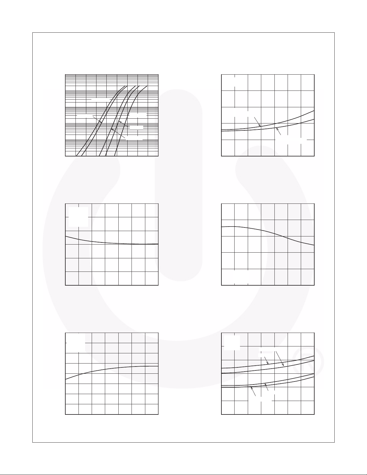
Fig. 1 Input Forward Current vs.
Forward Voltage
100
10
T
= 100°C
A
1
= -40°C
T
A
T
A
T
= 0°C
A
= 25°C
TA = 85°C
0.1
- Forward Current (mA)
F
I
0.01
0.001
0.8 0.9 1.0 1.1 1.2 1.3 1.4 1.5 1.6 1.7
VF - Forward Voltage (V)
Fig. 3 Low Level Output Voltage vs.
Ambient Temperature
0.6
VCC = 3.3V
= 2V
V
E
0.5
= 5mA
I
F
= 13mA
I
O
0.4
0.3
0.2
- Low Level Output Voltage (V)
0.1
OL
V
0.0
-40 -20 0 20 40 60 80 100
TA - Ambient Temperature (°C) TA - Ambient Temperature (°C)
Fig. 2 Input Threshold Current vs.
Ambient Temperature
2.5
VCC = 3.3V
V
= 0.6V
O
2.0
1.5
FOD060L
= 350Ω, 1kΩ, 4k Ω
R
L
1.0
0.5
- Input Threshold Current (mA)
TH
I
0.0
-40 -20 0 20 40 60 80 100
FOD260L
R
= 350Ω, 1kΩ, 4k Ω
L
TA - Ambient Temperature (°C)
Fig. 4 High Level Output Current
vs. Ambient Temperature
20
16
12
8
- High Level Output Current (nA)
4
VO = VCC = 3.3V
OH
I
= 2V
V
E
= 250 µA
I
F
0
-40 -20 0 20 40 60 80 100
Fig. 5 Low Level Output Current vs.
Ambient Temperature
40
VCC = 3.3V
V
= 2V
E
35
VOL = 0.6V
I
= 5mA
F
30
25
20
15
10
- Low Level Output Current (mA)
OL
5
I
0
-40 -20 0 20 40 60 80 100
T
- Ambient Temperature (°C)
A
- Propagation Delay (ns)
P
t
Fig. 6 Propagation Delay vs.
Ambient Temperature
80
VCC = 3.3V
= 7.5mA
I
F
70
R
= 350Ω
L
60
50
40
30
20
-40 -20 0 20 40 60 80 100
t
- FOD060L
PLH
- FOD260L
t
PLH
t
- FOD060L
PHL
- FOD260L
t
PHL
- Ambient Temperature (°C)
T
A
©2008 Fairchild Semiconductor Corporation www.fairchildsemi.com
FOD060L, FOD260L Rev. 1.0.5 5

Typical Performance Curves
FOD060L, FOD260L — 3.3V/5V High Speed-10 MBit/s Logic Gate Optocouplers
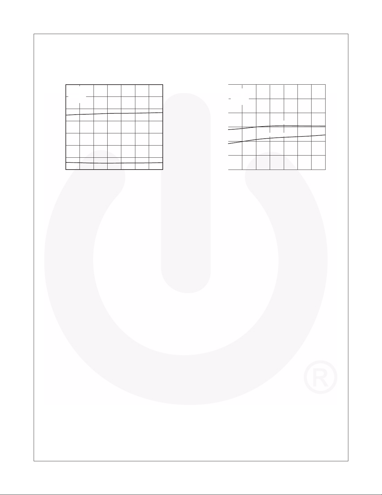
Fig. 7 Rise and Fall Times vs.
Ambient Temperature
35
VCC = 3.3V
= 7.5mA
I
F
30
RL = 350Ω
25
t
20
15
, - Rise, Fall Time (ns)
10
f
, t
r
t
5
0
-40 -20 0 20 40 60 80 100
r
tf
TA - Ambient Temperature (°C)
Fig. 8 Pulse Width Distortion vs.
Ambient Temperature
30
VCC = 3.3V
= 7.5mA
I
F
25
RL = 350Ω
20
15
10
5
PWD - Pulse Width Distortion (ns)
0
-40 -20 0 20 40 60 80 100
TA - Ambient Temperature (°C)
FOD260L
FOD060L
©2008 Fairchild Semiconductor Corporation www.fairchildsemi.com
FOD060L, FOD260L Rev. 1.0.5 6
 Loading...