

Fairchild FMBA06 service manual
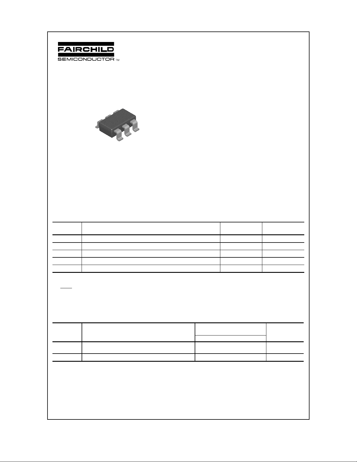
FMBA06
C2
E1
C1
B2
E2
B1
pin #1
SuperSOT-6
Mark: .1G
Dot denotes pin #1
NPN Multi-Chip General Purpose Amplifier
This device is designed for general purpose amplifier applications at collector
currents to 300 mA. Sourced from Process 33.
FMBA06
Absolute Maximum Ratings* T
= 25°C unless otherwise noted
A
Symbol Parameter Value Units
V
CEO
V
CBO
V
EBO
I
C
TJ, T
stg
Collector-Emitter Voltage 80 V
Collector-Base Voltage 80 V
Emitter-Base Voltage 4.0 V
Collector Current - Continuous 500 mA
Operating and Stora ge Junction Temperature Range -55 to +150
°
C
*These ratings are limiting values above which the serviceability of any semiconductor device may be impaired.
NOTES:
1) These ratings are based on a maximum junction temperature of 150 degrees C.
2) These are steady state limits. The factory should be consulted on applications involving pulsed or low duty cycle operations.
Thermal Characteristics T
= 25°C unless otherwise noted
A
Symbol Characteristic Max Units
FMBA06
P
D
R
JA
θ
Total Device Dissipation
Derate above 25°C
700
5.6
Thermal Resistance, Junction to Ambient 180
mW
mW/°C
C/W
°
4
1998 Fairchild Semiconductor Corporation
NPN Multi-Chip General Purpose Amplifier
(continued)
FMBA06
Electrical Characteristics T
= 25°C unless otherwise noted
A
Symbol Parameter Test Conditions Min Typ Max Units
OFF CHARACTERISTICS
V
(BR)CEO
V
(BR)EBO
I
CEO
I
CBO
Collector-Emitter Sustaining Voltage* IC = 1.0 mA, IB = 0 80 V
Emitter-Base B reak down Voltage
I
= 100 µA, IC = 0
E
4.0 V
Collector-Cutoff Current VCE = 60 V, IB = 0 0.1
Collector-Cutoff Current VCB = 80 V, IE = 0 0.1
µ
µ
ON CHARACTERISTICS
h
FE
V
V
sat
CE(
BE(on)
DC Current Gain IC = 10 mA, VCE = 1.0 V
= 100 mA, VCE = 1.0 V
I
Collector-Emi tter Saturation Volt age IC = 100 mA, IB = 10 mA 0.25 V
)
C
Base-Emit t er On Voltage IC = 100 mA, VCE = 1.0 V 1.2 V
100
100
SMALL SIGNAL CHARACTERISTICS
f
T
Current Gain - Bandwidth Product IC = 10 mA, VCE = 2.0 V,
f = 100 MHz
100 MHz
*Pulse T est: Pulse Width ≤ 300 µs, Duty Cycle ≤ 2.0%
A
A
Spice Model
NPN (Is=8.324f Xti=3 Eg=1.11 Vaf=100 Bf=12.16K Ne=1.368 Ise=73.27f Ikf=.1096 Xtb=1.5 Br=11.1 Nc=2 Isc=0
Ikr=0 Rc=.25 Cjc=18.36p Mjc=.3843 Vjc=.75 Fc=.5 Cje=55.61p Mje=.3834 Vje=.75 Tr=72.15n Tf=516.1p Itf=.5
Vtf=4 Xtf=6 Rb=10)
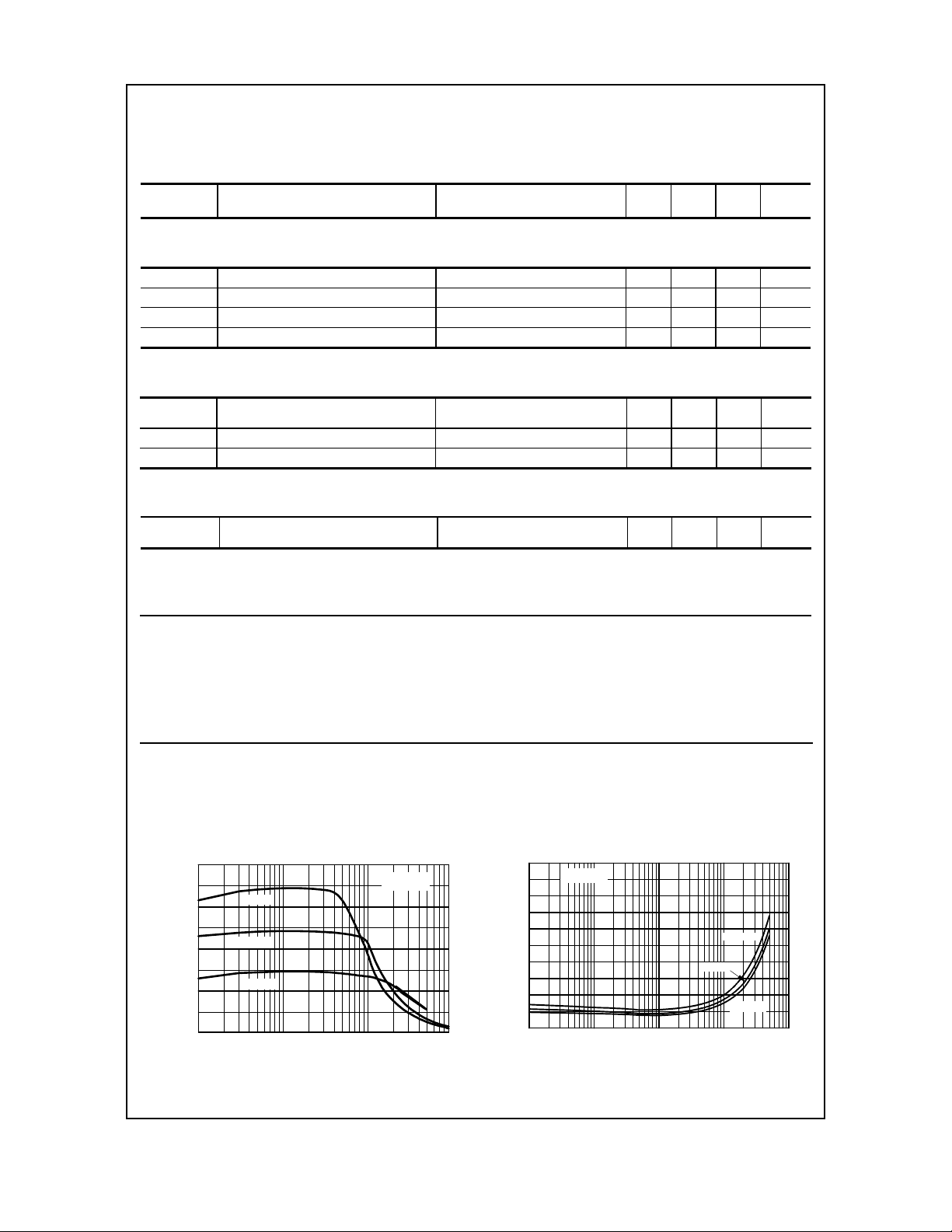
T ypical Characteristics
Typica l P uls ed Curre nt G a in
vs Collector Current
200
150
100
50
FE
0.001 0.01 0.1
h - TYPICAL PULSED CURRENT GAIN
125 °C
25 °C
- 40 °C
I - COLLECTOR CURRENT (A)
C
V = 1V
CE
Co llecto r -Emitter Sa turati o n
Voltag e vs Coll ector Cur rent
0.5
0.4
0.3
0.2
0.1
0
0.1 1 1 0 100 1 000
CE SAT
V - COL LEC TOR EMITTER VOLTA G E ( V)
= 10
β
25 °C
I - COLLECTOR CURRENT (mA)
C
125 °C
- 40 °C
 Loading...