

Fairchild FM27C512 service manual
查询FM27C512供应商查询FM27C512供应商
January 2000
FM27C512
524,288-Bit (64K x 8) High Performance CMOS EPROM
FM27C512 524,288-Bit (64K x 8) High Performance CMOS EPROM
General Description
The FM27C512 is a high performance 512K UV Erasable Electrically Programmable Read Only Memory (EPROM). It is manufactured using Fairchild’s proprietary CMOS AMG™ EPROM technology for an excellent combination of speed and economy while
providing excellent reliability.
The FM27C512 provides microprocessor-based systems storage
capacity for portions of operating system and application software. Its 90 ns access time provides no wait-state operation with
high-performance CPUs. The FM27C512 offers a single chip
solution for the code storage requirements of 100% firmwarebased equipment. Frequently-used software routines are quickly
executed from EPROM storage, greatly enhancing system utility.
The FM27C512 is configured in the standard JEDEC EPROM
pinout which provides an easy upgrade path for systems which are
currently using standard EPROMs.
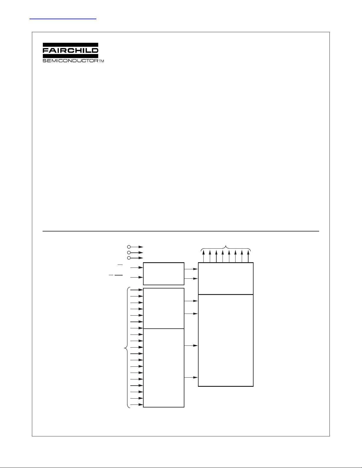
Block Diagram
V
CC
GND
V
PP
OE
CE/PGM
Output Enable and
Chip Enable Logic
The FM27C512 is one member of a high density EPROM Family
which range in densities up to 4 Megabit.
Features
■ High performance CMOS
— 90 ns access time
■ Fast turn-off for microprocessor compatibility
■ Manufacturers identification code
■ JEDEC standard pin configuration
— 28-pin PDIP package
— 32-pin chip carrier
— 28-pin CERDIP package
Data Outputs O0 - O
Output
Buffers
7
A0 - A
Address
AMG is a trademark of WSI, Inc.
© 1998 Fairchild Semiconductor Corporation
FM27C512
Inputs
1
. . . . . . . . .
524,288-Bit
Cell Matrix
DS800035-1
www.fairchildsemi.com
www.fairchildsemi.com
Y Decoder
15
X Decoder
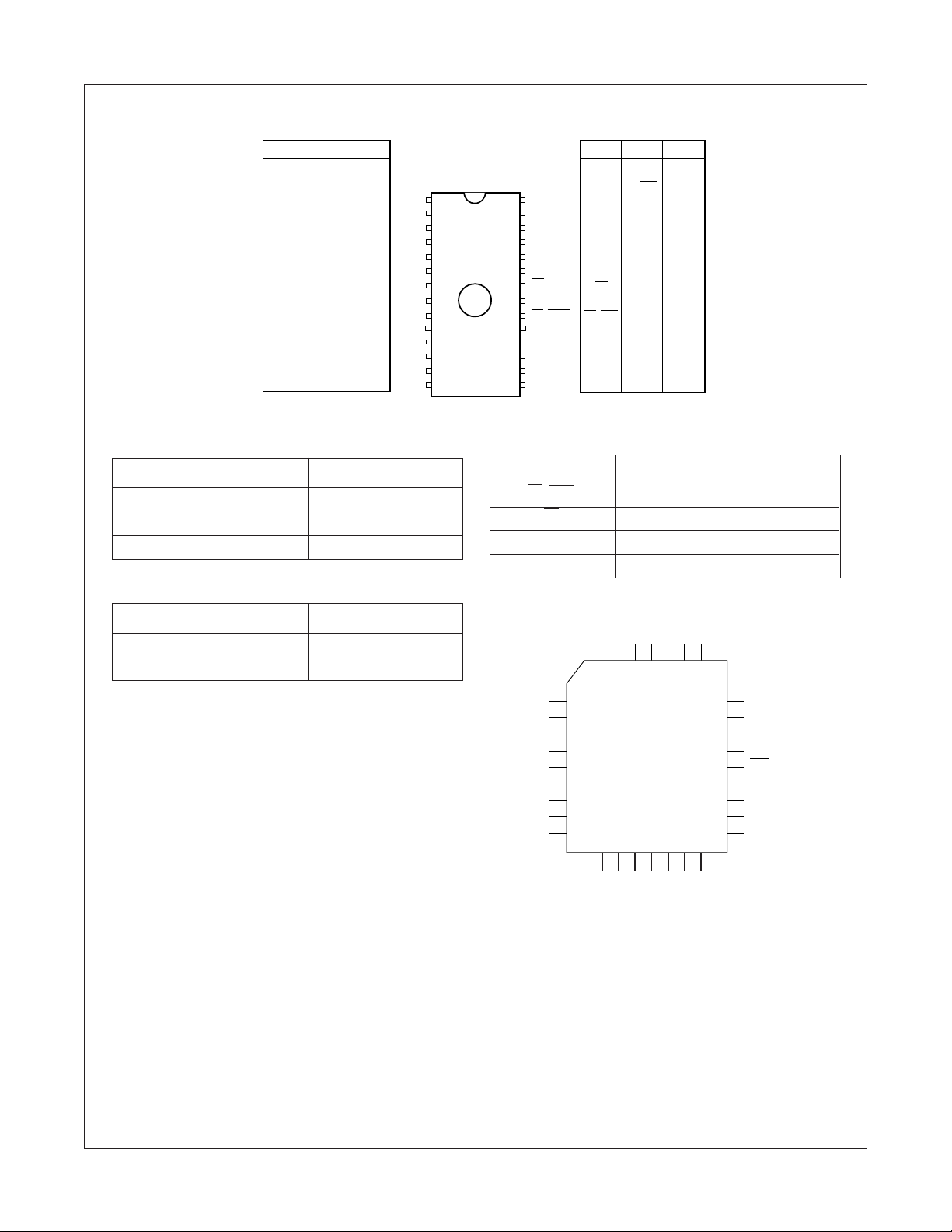
Connection Diagrams
FM27C512 524,288-Bit (64K x 8) High Performance CMOS EPROM
27C040 27C010 27C256
XX/
XX/
V
V
PP
A
16
A
15
A
12
A
A
A
A
A
A
A
A
O
O
O
GND
Compatible EPROM pin configurations are shown in the blocks adjacement to the FM27C512 pins.
PP
A
16
A
V
15
PP
A
A
A
12
A
7
7
A
6
6
A
5
5
A
4
4
A
3
3
A
2
2
A
1
1
A
0
0
O
0
0
O
1
1
O
2
2
GND
GND
15
12
A
12
A
7
A
A
A
A
A
A
A
A
O
O
O
7
6
A
6
5
A
5
4
A
4
3
A
3
2
A
2
1
A
1
0
A
0
0
O0
1
O
1
2
O
2
GND
Commercial Temp Range (0°C to +70°C)
DIP
FM27C512
1
2
3
4
5
6
7
8
9
10
11
12
13
14
Pin Names
28
27
26
25
24
23
22
21
20
19
18
17
16
15
Parameter/Order Number Access Time (ns)
FM27C512 Q, N, V 90 90
FM27C512 Q, N, V 120 120
FM27C512 Q, N, V 150 150
Industrial Temp Range (-40°C to +85°C)
Parameter/Order Number Access Time (ns)
FM27C512 QE, NE, VE 120 120
FM27C512 QE, NE, VE 150 150
27C256 27C010 27C040
V
V
CC
A
14
A
13
A
8
A
9
A
11
OE/V
PP
A
10
CE/PGM
O7
O
6
O
5
O4
O
3
V
CC
A
14
A
13
A
8
A
9
A
11
OE
A10
CE/PGM
O7
O
6
O
5
O4
O
3
V
XX/PGM
XX
A
A
A
A
A
OE
A10
CE
O7
O
O
O4
O
CC
CC
A
18
A
17
A
14
14
A
13
13
A
8
8
A
9
9
A
11
11
OE
A10
CE/PGM
O7
O
6
6
O
5
5
O4
O
3
3
A0–A15 Addresses
CE/PGM Chip Enable/Program
OE Output Enable
O0–O7 Outputs
NC Don’t Care (During Read)
PLCC
A7
A12
A15NCVCC
4 3 2 1 32 31 30
A14
A13
DS800035-2
Q = Quartz-Windowed Ceramic DIP Package
N = Plastic DIP Package
V = PLCC Package
• All packages conform to the JEDEC standard.
• All versions are guaranteed to function for slower speeds.
A6
A5
A4
A3
A2
A1
A0
NC
O0
5
6
7
8
9
10
11
12
13
14 15 16 17 18 19 20
O1
O2
GND
O3O4O5
NC
29
28
27
26
25
24
23
22
21
A8
A9
A11
NC
OE/VPP
A10
CE/PGM
O7
O8
DS800035-3
FM27C512
2
www.fairchildsemi.com
www.fairchildsemi.com
FM27C512 524,288-Bit (64K x 8) High Performance CMOS EPROM
Absolute Maximum Ratings (Note 1)
Storage Temperature -65°C to +150°C
All Input Voltages Except A9 with
Respect to Ground -0.6V to +7V
VPP and A9 with Respect to Ground -0.7V to +14V
Supply Voltage with
V
CC
Respect to Ground -0.6V to +7V
ESD Protection
(MIL Std. 883, Method 3015.2) >2000V
All Output Voltages with
Respect to Ground V
+ 1.0V to GND -0.6V
CC
Operating Range
Range Temperature V
Commercial 0°C to +70°C +5V ±10%
CC
Tolerance
Industrial -40°C to +85°C +5V ±10%
Read Operation
DC Electrical Characteristics
Symbol Parameter Test Conditions Min Max Units
V
V
V
V
I
I
I
CC1
I
CC2
I
V
I
SB1
SB2
PP
I
LO
IL
IH
OL
OH
PP
LI
Input Low Level -0.5 0.8 V
Input High Level 2.0 VCC +1 V
Output Low Voltage IOL = 2.1 mA 0.4 V
Output High Voltage IOH = -2.5 mA 3.5 V
VCC Standby Current (CMOS) CE = VCC ±0.3V 100 µA
VCC Standby Current CE = V
IH
VCC Active Current CE = OE = V
IL
f = 5 MHz 40 mA
1mA
VCC Active Current CE = GND, f = 5 MHz
CMOS Inputs Inputs = VCC or GND, I/O = 0 mA 35 mA
C, E Temp Ranges
VPP Supply Current VPP = V
CC
VPP Read Voltage VCC - 0.7 V
10 µA
CC
Input Load Current VIN = 5.5V or GND -1 1 µA
Output Leakage Current V
= 5.5V or GND -10 10 µA
OUT
V
AC Electrical Characteristics
Symbol Parameter 90 120 150 Units
Min Max Min Max Min Max
FM27C512
t
ACC
t
t
t
t
CE
OE
DF
OH
Address to Output Delay 90 120 150 ns
CE to Output Delay 90 120 150
OE to Output Delay 40 50 50
Output Disable to 35 25 45
Output Float
Output Hold from Addresses, CE or OE, 0 0 0
Whichever Occurred First
3
www.fairchildsemi.com
www.fairchildsemi.com
 Loading...