Fairchild FL7701 service manual

www.fairchildsemi.com
AN-9744
Smart LED Lamp Driver IC with PFC Function
Introduction
The FL7701 is a PWM peak current controller for a buck
converter topology operating in Continuous Conduction
Mode (CCM) with an intelligent PFC function using a
digital control algorithm. The FL7701 has an internal selfbiasing circuit that is a current source using a high-voltage
switching device. When the input voltage is applied to the
HV pin is over 25V to 450V, the FL7701 maintains a
15.5V
block for stable operation. When the V
higher than V
the V
at the VCC pin. The FL7701 also has a UVLO
DC
voltage reaches
CC
, the UVLO block starts operation.hen
CCST+
drops below the V
CC
IC operation stops.
CCST-,
Hysteresis is provided for stable operation of the IC when
input the voltage is in noisy circumstances or unstable
conditions. The FL7701 has a “smart” internal block for AC
input condition. If an AC source with 50Hz or 60Hz is
applied, the IC automatically changes the internal reference
to adjust to input conditions with an internal fixed transient
time. When a DC source connects to the IC, the internal
reference immediately changes to DC waveform.
V
HV
Device
Q
sup
Driver
I
line
FL7701
V
CC
DSG
C
DAC_OUT
Reference
ZCD_OUT
VSUP_SEN
DSG: Digital Sine-Wave Generator
HV Device : High-Voltage Device
S
R
HV
OUT
CS
+ V
LED
I
sw
GND
-
L
LED Load
IL
D1
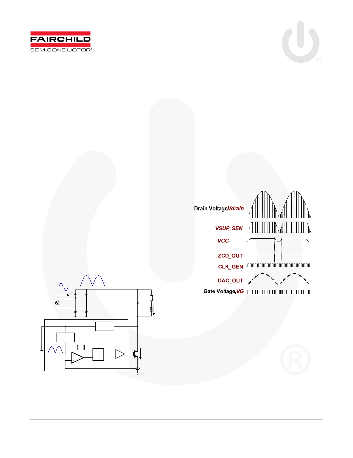
Figure 1. Basic Block of FL7701
The internal DAC_OUT reference signal is dependent on
the V
voltage. Using the DAC_OUT signal and internal
CC
clock, CLK_GEN; the FL7701 automatically makes a
digital reference signal, DAC_OUT. If the FL7701 cannot
detect the ZCD_OUT signal, the IC has an abnormal
internal reference signal. In this situation, this phenomenon
causes a lighting flicker.
Figure 2. FL7701 Operation
Soft-Start Function
The FL7701 has an internal soft-start to reduce inrush
current at IC startup. When the IC starts operation, the
internal reference of the IC slowly increases up to a fixed
level for around seven cycles. After settling down this
transient period, the internal reference is fixed at a certain
DC level. In this time, the IC continually tries to find input
phase information from the VCC pin. If the IC succeeds in
getting phase information from the VCC, the IC
automatically follows a similar shape reference, which it
made during the transient times, seven periods. If not, the
IC has a DC reference level.
© 2011 Fairchild Semiconductor Corporation www.fairchildsemi.com
Rev. 1.0.0 • 10/11/11

AN-9744 APPLICATION NOTE
To precisely and reliably calculate the input voltage phase
on the VCC pin, the FL7701 uses a digital technique
(sigma/delta modulation/demodulation). After finishing this
digital technique, the FL7701 has new reference that is the
same phase as input voltage, as shown in Figure 6.
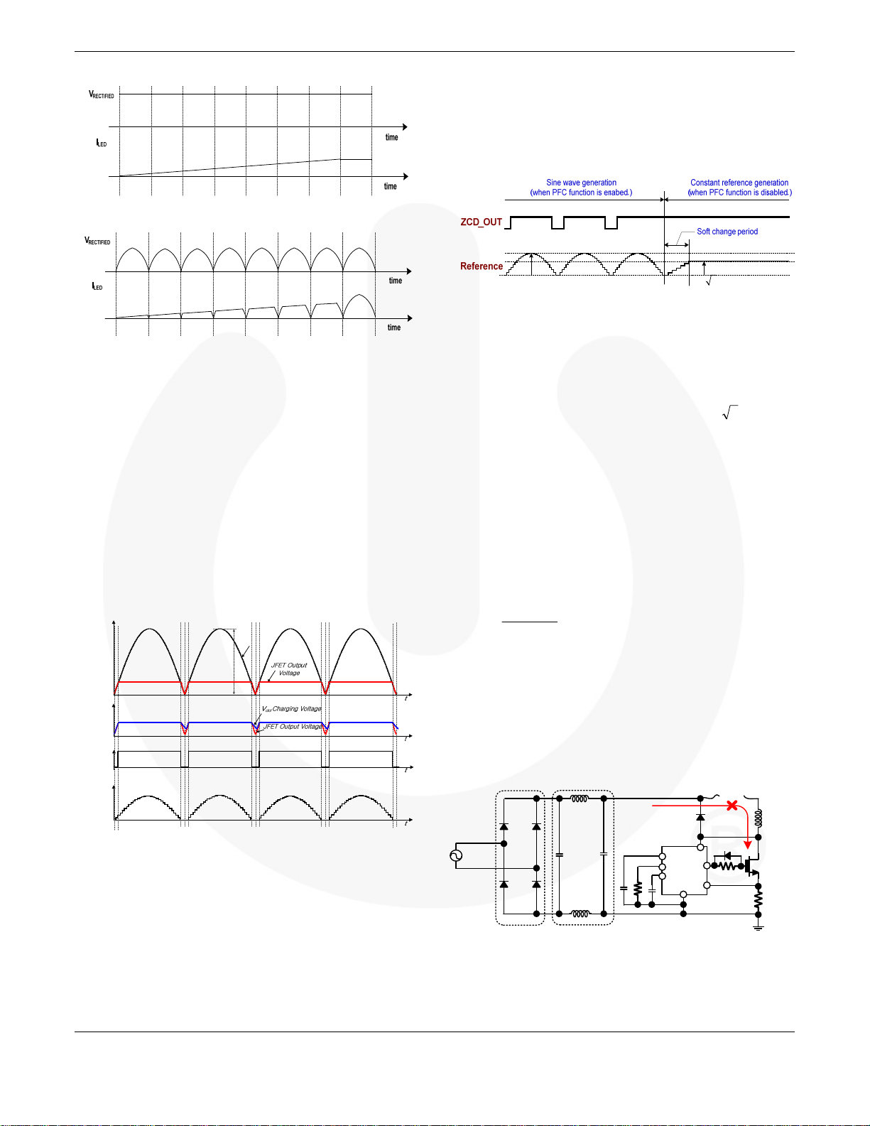
Figure 3. DC Input Condition
Figure 4. AC Input Condition
Internal Power Factor (PF) Function
The FL7701 application circuit does not use the input
electrolytic capacitor for voltage rectification after a bridge
diode because this system design results in a high pulse
shape input current. This pulse shape current contains many
harmonic components, so the total system cannot have high
PF. To get high PF performance, the FL7701 uses a
different approach.
The FL7701 has an intelligent internal PFC function that
does not require additional detection pins or other
components. The IC does not need a bulk capacitor on the
VCC pin for supply voltage stabilization.
V
bridge
Input Voltage
Peak
Bridge Diode
Output Voltage
Vp
/2Vp
Figure 6. Internal Reference
This signal enters the final comparator and current
information from the sensing resistor. Pin 1 is compared. As
a result, the FL7701 has a high power factor and can
operate as a normal peak current controller as shown in
Figure 6, in the DC input condition. The relationship
between AC Input Mode and DC Input Mode is
.
2
Output Frequency Programming
The FL7701 can program output frequency using an RT
resistor or with the RT pin in open condition. The FL7701
can have a fixed output frequency around 45kHz when the
RT pin is left open. For increasing system reliability, a
small-value capacitor is recommended below 100nF in RTopen condition. The relationship between output frequency
and the RT resistor is:
9
1002.2
f
OSC
[Hz]
RT
(1)
Output Open-Circuit Protection
VCC
The recommended connection method is shown in Figure 7.
The FL7701 has a high-voltage power supply circuit, which
self biases using high-voltage process device. If the LED
ZCD
DAC_OUT
Figure 5. Internal PFC Function
The FL7701 detects the VCC changing point for making the
Zero Crossing Detection (ZCD) signal, which is an internal
timing signal for making DAC_OUT. Normally, a capacitor
does not connect to the chip, the IC cannot start.
BD
EMI filter
L1
C1
L2
C2
ADIM
RT
VCC
R3
C3
C4
D1
HV
FL7701
GND
OUT
LED
L
D2
R1
CS
R2
connected to the VCC pin is used for voltage stabilization
and acts as low-pass filter or noise-canceling filter. This
increases the ability to get a stable timing signal at the VCC
Figure 7. LED Open Condition
pin, even is there may be noise on other pins.
© 2011 Fairchild Semiconductor Corporation www.fairchildsemi.com
Rev. 1.0.0 • 10/11/11 2

AN-9744 APPLICATION NOTE
Inductor Short-Circuit Protection
The FL7701 has an Abnormal Over-Current Protection
(AOCP) function. If the voltage of the LED current-sensing
resistor is higher than 2.5V, even within Leading EdgeBlanking (LEB) time of 350ns; the IC stops operation.
VCC
RT OUT
GND
VCC
ZCD
Oscillator
time
ZCD
DAC
Soft start
Digital Block
Reference
UVLO
TSD
-
+
LEB
Leading Edge
Blanking
JFET
S
Q
R
-
+
AOCP
2.5V
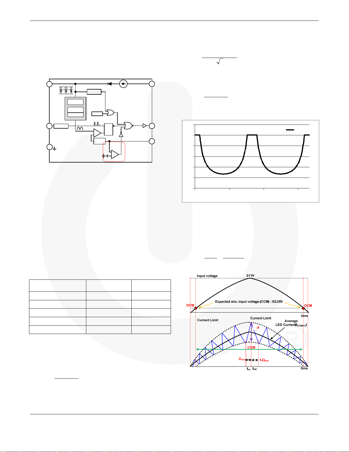
Figure 8. AOCP Function
HV
CS
Analog Dimming Function
The Analog Dimming (ADIM) function adjusts the output
LED current by changing the voltage level of the ADIM pin.
Application Information
The FL7701 is an innovative buck converter control IC
designed for LED applications. It can operate from DC and
AC input voltages without limitation and its input voltage
level can be up to 305V
Table 1 shows one example of a design target using the
FL7701 device.
or 400VDC.
AC
For example, if V
= 220V and ten LEDs are in series
IN(max)
connection, the minimum duty ratio is:
5.310
D
min
220285.0
132.0
Step 2: Maximum Duty Ratio
Similar to Step 1, calculate maximum duty ratio as:
nV
D
max
F
V
in
(min)
(3)
60
[%]
50
40
30
20
10
0
051015
Duty
[ms]
Figure 9. Duty Variation vs. Time
The FL7701 has a 50% maximum duty cycle to prevent
sub-harmonic instability. Assume the minimum input
voltage enters 50% duty ratio. Using Equation 2, recalculate the minimum input voltage for CCM operation:
nV
F
V
in
(min)
D
35
5.085.0
][35.82
V
(4)
Table 1. Target Design Specification
Item Specification Note
Frequency 45kHz
Output Voltage 35 VF=3.5V,
Output LED Current 0.3 rms
Output LED Current 0.5 Peak
Input Voltage (Max.) 220 V
AC(rms)
Step 1: Minimum Duty Ratio
The FL7701 has a fixed internal duty ratio range between
2% and 50%. This range depends on the input voltage and
the number of LEDs in the string.
nV
F
D
min
V
(max)
in
(2)
Figure 10. Estimated Waveforms
where η is efficiency of system; V
input voltage; V
is forward-drop voltage of LED; and n
F
is maximum
IN(max)
is LED number in series connection.
© 2011 Fairchild Semiconductor Corporation www.fairchildsemi.com
Rev. 1.0.0 • 10/11/11 3
 Loading...