Fairchild FKN08PN60S service manual

FKN08PN60S
TRIAC (Silicon Bidirectional Thyristor)
Application Explanation
• Switching mode power supply, light dimmer, electric flasher unit, hair drier
• TV sets, stereo, refrigerator, washing machine
• Electric blanket, solenoid driver, small motor control
• Photo copier, electric tool
3
1
1 2 3
TO-92
FKN08PN60S — TRIAC (Silicon Bidirectional Thyristor)
February 2008
1: T
1
2: Gate
3: T
2
2
Absolute Maximum Ratings T
= 25°C unless otherwise noted
a
Symbol Parameter Value Rating Units
V
DRM
V
RRM
I
T (RMS)
I
TSM
I2t I2t for Fusing Value corresponding to halfwave,
P
GM
P
G (AV)
V
GM
I
GM
T
J
T
STG
Peak Repetitive Off-State Voltage
Sine Wave 50 to 60Hz, Gate Open
RMS On-State Current Commercial frequency, sine full wave
600 V
0.8 A
360° conduction, Tc= 70℃
Surge On-State Current Sinewave half cycle, peak value,
60Hz 8 A
non-repetitive
0.26 A2s
surge on-state current, tp=8.33ms
Peak Gate Power Dissipation 5 W
Average Gate Power Dissipation 0.1 W
Peak Gate Voltage 5 V
Peak Gate Current 1 A
Junction Temperature - 40 ~ 125 °C
Storage Temperature - 40 ~ 125 °C
Thermal Characteristics
Symbol Parameter Value Units
R
θJC
R
θJA
Note1: Infinite cooling condition.
Note2: JESD51-10 ( Test Borad: FR4 3.0”*4.5”*0.062”, Minimum land pad)
Thermal Resistance, Junction to Case
Thermal Resistance, Junction to Ambient
(note1)
(note2)
45
160
°C/W
°C/W
© 2007 Fairchild Semiconductor Corporation www.fairchildsemi.com
FKN08PN60S Rev. 1.0.0 1

FKN08PN60S — TRIAC (Silicon Bidirectional Thyristor)
Electrical Characteristics T
= 25°C unless otherwise noted
C
Symbol Parameter Test Condition
I
DRM
I
RRM
V
TM
V
GT
I
GT
V
GD
I
H
I
L
dv/dt(s) Critical Rate of Rise of
dv/dt(c) Critical-Rate of Rise of Off-State Com-
Repetieive Peak Off-State Current V
DRM/VRRM
applied - - 100 μA
On-State Voltage TC=25°C, ITM=1.12A
Instantaneous measurement
Gate Trigger Voltage
(Note 2)
I
VD=12V , RL=100Ω
II T2(+), Gate (-) - - 2.0 V
III T2(-), Gate (-) - - 2.0 V
Gate Trigger Current
(Note 2)
I
VD=12V , RL=100Ω
II T2(+), Gate (-) - - 5 mA
III T2(-), Gate (-) - - 5 mA
Gate Non-Trigger Voltage TJ=125°C, VD=1/2V
DRM
Holding Current (I, II,III) VD = 12V, ITM = 200mA - - 15 mA
Latching Current I, III VD = 12V, IG = 10mA - - 15 mA
II - - 20 mA
V
= 63% Rated, Tj = 125°C,
Off-State Voltag
DRM
Exponential Rise
mutating Voltage (di/dt=-0.7A/uS)
Commutation dv/dt test
Min. Typ. Max. Units
- - 1.8 V
T2(+), Gate (+) - - 2.0 V
T2(+), Gate (+) - - 5 mA
0.2 - - V
20 - - V/μs
3.0 - - V/μs
V
DRM
(V)
Test Condition
FKN08PN60S 1. Junction Temperature
TJ=125°C
2. Rate of decay of on-state
commutating current (di/dt)C
3. Peak off-state voltage
VD = 300V
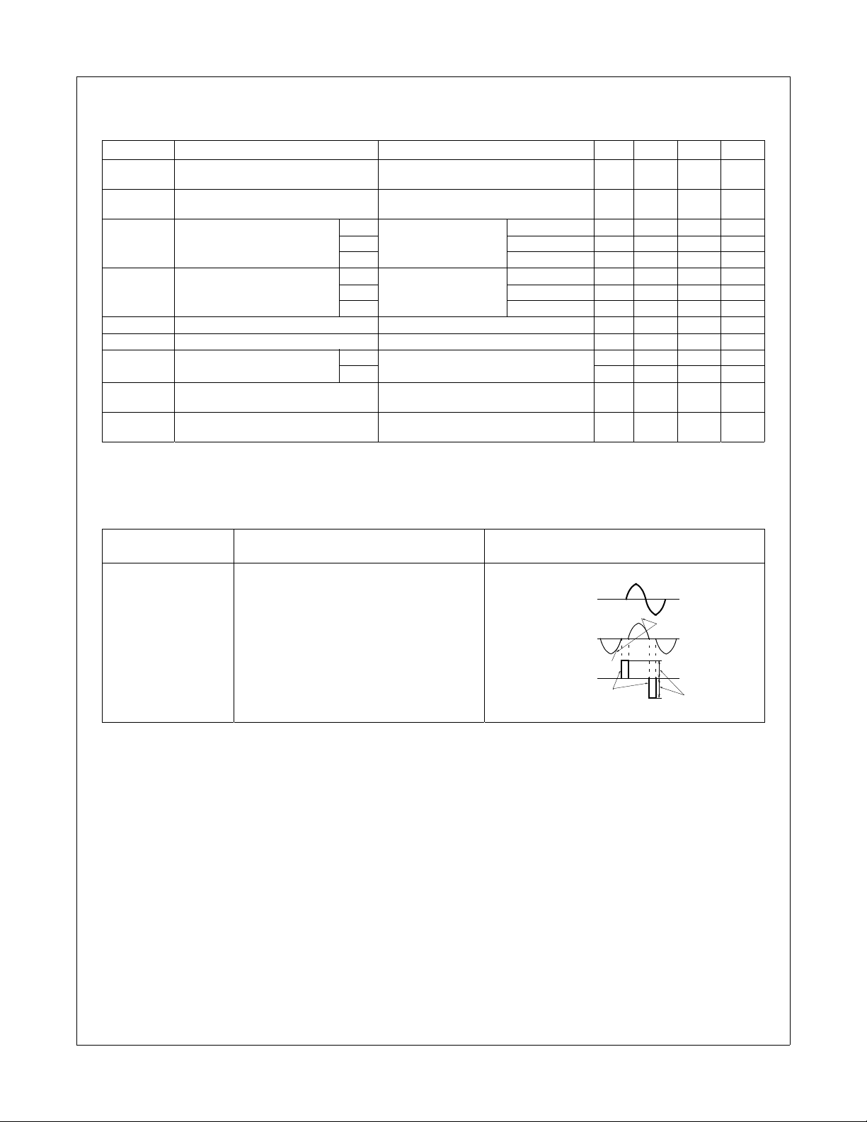
Commutating voltage and current waveforms
(inductive load)
Supply Voltage
Main Current
Main Voltage
(dv/dt)
C
(di/dt)
Time
C
Time
Time
V
D
© 2007 Fairchild Semiconductor Corporation www.fairchildsemi.com
FKN08PN60S Rev. 1.0.0 2

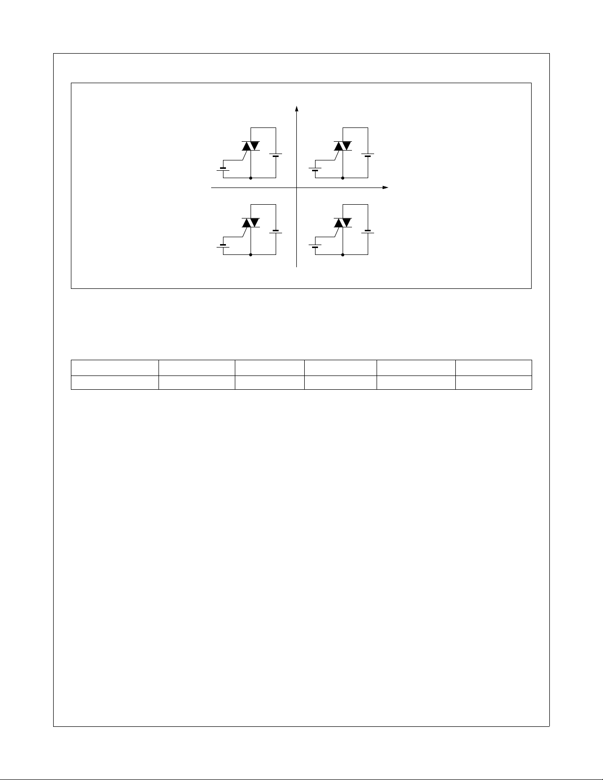
Quadrant Definitions for a Triac
FKN08PN60S — TRIAC (Silicon Bidirectional Thyristor)
T2 Positive
+
(+) I
GATE
(+) I
GATE
(+) T2
GT
T1
GT
(-) T2
GT
T1
(+) T2
Quadrant II Quadrant I
Quadrant III Quadrant IV
(-) I
GT
GATE
T1
IGT -+ I
(-) T2
(-) I
GT
GATE
T1
-
T2 Negative
Package Marking and Ordering Information
Device Marking Device Package Packing Tape Width Quantity
K08PN60S FKN08PN60S TO-92 BULK -- --
© 2007 Fairchild Semiconductor Corporation www.fairchildsemi.com
FKN08PN60S Rev. 1.0.0 3
 Loading...