FHP3130, FHP3230, FHP3430
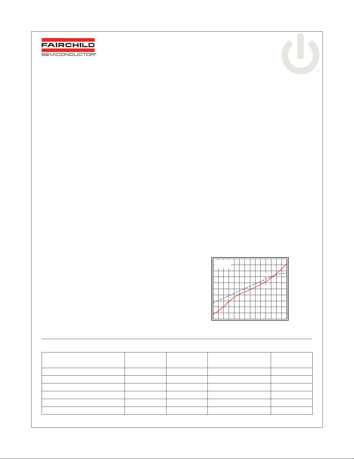
0.01
Differential Gain (%)
-0.7 -0.5 -0.3 -0.1 0.1 0.3 0.5 0.7
Input Voltage (V)
-0.01
-0.006
-0.004
-0.002
0
0.002
0.004
0.006
0.008
-0.008
0.01
Differential Phase (deg)
-0.01
-0.006
-0.004
-0.002
0
0.002
0.004
0.006
0.008
-0.008
Vs = ±5V
RL = 150Ω
Gain
Phase
Single, Dual, and Quad, High-Speed, 2.7V to 12V,
Rail-to-Rail Ampliers
FHP3130, FHP3230, FHP3430 Single, Dual, and Quad, High-Speed, 2.7V to 12V, Rail-to-Rail Ampliers
October 2006
Features at ±5V
2.5mA supply current per amplier
■
0.008%/0.01° differential gain/phase
■
10MHz 0.1dB bandwidth
■
Output voltage range at RL = 150W: -4.8V to 4.8V
■
Input includes negative rail
■
110V/µs slew rate
■
±100mA output current
■
17nV/√Hz input voltage noise
■
>100dB PSRR, CMRR, and open-loop gain
■
FHP3130 – improved replacement for KM4100
■
FHP3230 – improved replacement for KM4200
■
FHP3130 lead-free package options
■
(SOT23-5, SOIC-8)
FHP3230 lead-free package options
■
(MSOP-8, SOIC-8)
FHP3430 lead-free package options
■
(TSSOP-14, SOIC-14)
RoHS compliant
■
Fully specied at +3V, +5V, and ±5V supplies
■
Applications
A/D driver
■
Active lters
■
CCD imaging systems
■
CD/DVD ROM
■
Coaxial cable drivers
■
Portable/battery-powered applications
■
Twisted-pair driver
■
Video driver
■
Description
The FHP3130 (single), FHP3230 (dual), and FHP3430
(quad) are low-cost, high-performance, voltage feedback
ampliers that consume only 2.5mA of supply current per
channel, while providing ±100mA of output current. These
ampliers are designed to operate from 2.7V to 12V (±6V)
supplies. The common mode voltage range includes the
negative rail and the output provides rail-to-rail performance.
The FHP3130, FHP3230, and FHP3430 are designed on
a complimentary bipolar process and provide 170MHz of
bandwidth and 110V/µs of slew rate at a supply voltage of
±5V. The combination of low power, rail-to-rail performance,
low-voltage operation, and tiny package options make
these ampliers well suited for use in many general-
purpose, high-speed applications.
These ampliers also provide excellent video specications.
They offer extremely low differential gain and phase
(0.008%/0.01°) and 0.1dB gain atness to 10MHz for
superb standard denition video performance. Their output
drive capability effortlessly supports four video loads.
Ordering Information
Part Number
FHP3130IS5X
FHP3130IM8X SOIC-8 Yes -40°C to +85°C Reel
FHP3230IMU8X MSOP-8 Yes -40°C to +85°C Reel
FHP3230IM8X SOIC-8 Yes -40°C to +85°C Reel
FHP3430IMTC14X TSSOP-14 Yes -40°C to +85°C Reel
FHP3430IM14X SOIC-14 Yes -40°C to +85°C Reel
Moisture sensitivity level for all parts is MSL-1.
© 2006 Fairchild Semiconductor Corporation www.fairchildsemi.com
FHP3130, FHP3230, FHP3430 Rev. 3.0.2
Package Pb-Free
Operating
Temperature Range
Packaging
Method
SOT23-5 Yes -40°C to +85°C Reel
2
3
4 5
6
7
8
-Vs
+Vs
+IN1
NC
OUT
NC
1
-IN1
NC
FHP3130
SOIC
-
+
2
3
5
4
+IN
+Vs
-IN
1
-Vs
OUT
FHP3130
SOT23
7
2
3
4
-Vs
+IN1
1
-IN1
OUT1
FHP3230
SOIC/MSOP
5
6
7
8
OUT2
+Vs
-IN2
+IN2
4
2
3
4
11
12
13
14
+Vs
-IN4
+IN1
OUT4
+IN4
-Vs
1
-IN1
OUT1
FHP3430
SOIC/TSSOP
5
6
7
OUT2
-IN2
+IN2
8
9
10
+IN3
-IN3
OUT3
Typical Application - YC Video Line Driver
FHP3130, FHP3230, FHP3430 Single, Dual, and Quad, High-Speed, 2.7V to 12V, Rail-to-Rail Ampliers
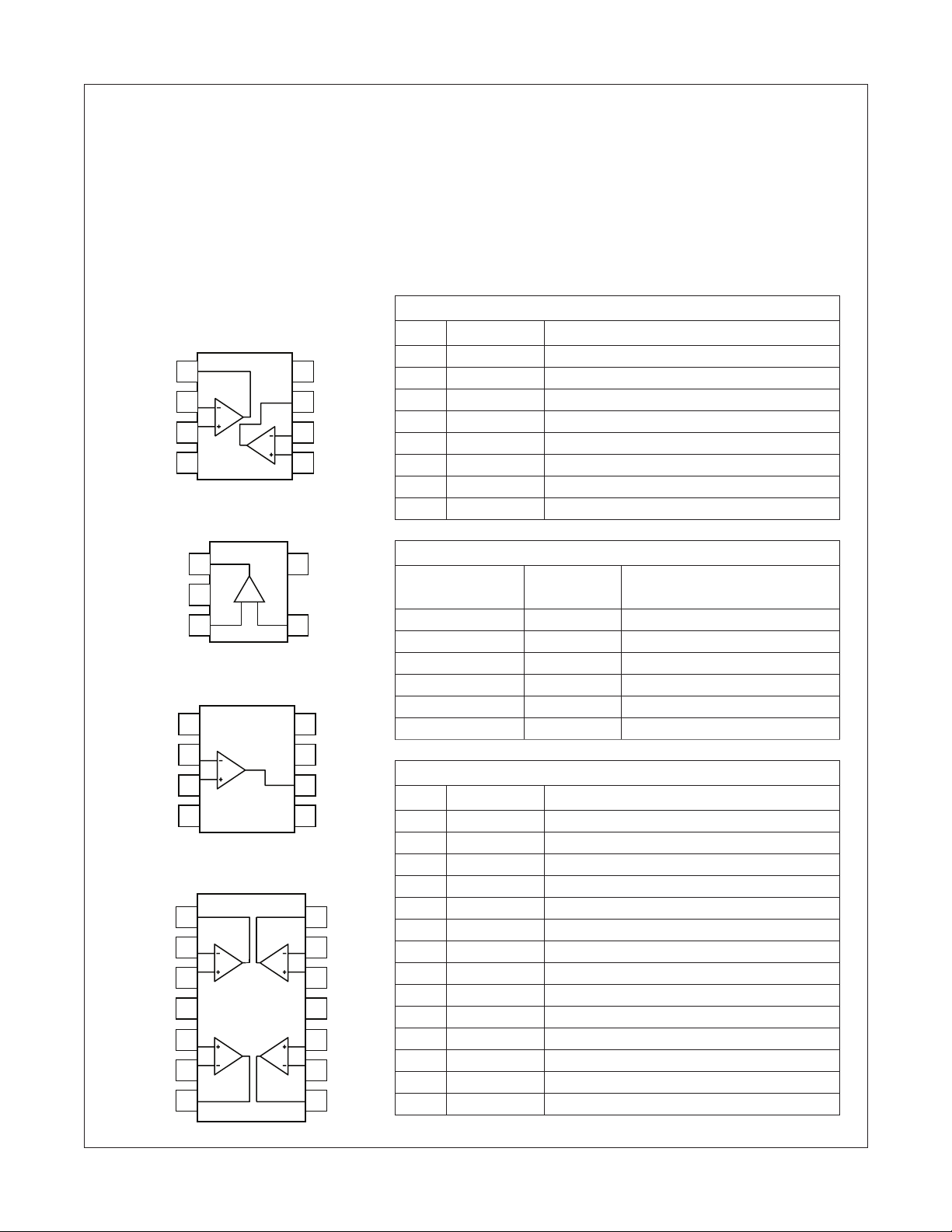
Pin Congurations
Pin Assignments
FHP3230
Pin # Name Description
1 OUT1 Output, channel 1
2 -IN1 Negative Input, channel 1
3 +IN1 Positive Input, channel 1
4 -Vs Negative supply
5 +IN2 Positive Input, channel 2
6 -IN2 Negative Input, channel 2
7 OUT2 Output, channel 2
8 +Vs Positive supply
FHP3130
Pin #
SOT/SOIC Name Description
1 / 6 OUT Output
2 / 4 -Vs Negative supply
3 / 3 +IN Positive Input
4 / 2 -IN Negative Input
5 / 7 +Vs Positive supply
na / 1, 5, 8 NC No Connect
FHP3430
Pin # Name Description
1 OUT1 Output, channel 1
2 -IN1 Negative Input, channel 1
3 +IN1 Positive Input, channel 1
4
© 2006 Fairchild Semiconductor Corporation 2 www.fairchildsemi.com
FHP3130, FHP3230, FHP3430 Rev. 3.0.2
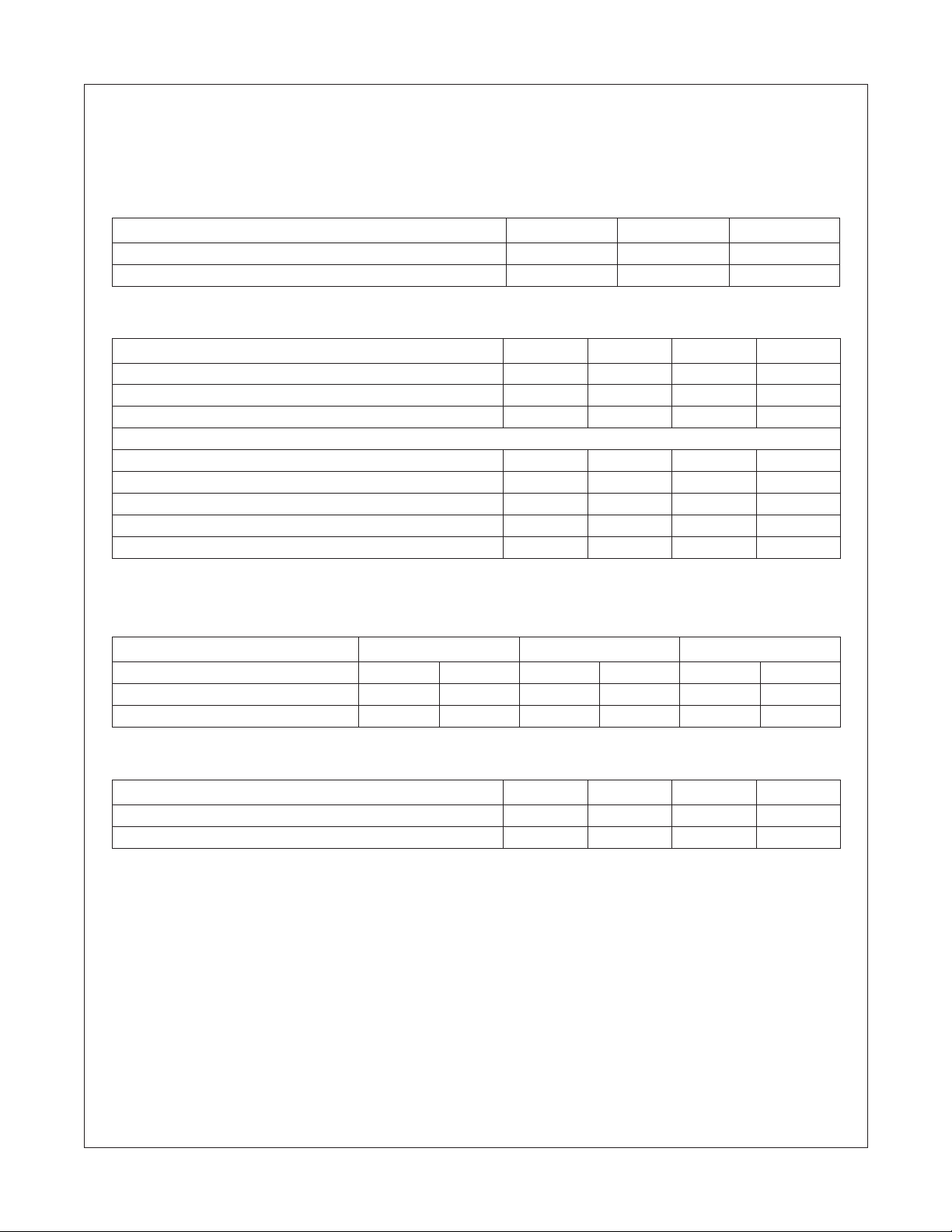
Absolute Maximum Ratings
The “Absolute Maximum Ratings” are those values beyond which the safety of the device cannot be guaranteed. The
device should not be operated at these limits. The parametric values dened in the Electrical Characteristics tables are
not guaranteed at the absolute maximum ratings. The “Recommended Operating Conditions” table denes the conditions
for actual device operation.
Parameter Min. Max. Unit
Supply Voltage 0 13.3 V
Input Voltage Range -V
-0.5V +V
s
+0.5V V
s
Reliability Information
Parameter Min. Typ. Max. Unit
Junction Temperature 150 °C
Storage Temperature Range -65 150 °C
Lead Temperature (Soldering, 10s) 300 °C
Thermal Resistance
8-Lead SOIC
8-Lead MSOP
5-Lead SOT23
14-Lead TSSOP
14-Lead SOIC
Notes:
Package thermal resistance (qJA), JDEC standard, multi-layer test boards, still air.
1.
(1)
(1)
(1)
(1)
(1)
155 °C/W
246 °C/W
296 °C/W
140 °C/W
128 °C/W
FHP3130, FHP3230, FHP3430 Single, Dual, and Quad, High-Speed, 2.7V to 12V, Rail-to-Rail Ampliers
ESD Protection
Product FHP3130 FHP3230 FHP3430
Package SOT23 SOIC SOIC MSOP SOIC TSSOP
Human Body Model (HBM) 3.5kV >4kV 3.5kV 3.5kV 3kV 5kV
Charged Device Model (CDM) >2kV >2kV 2kV 1.5kV 2kV 1.5kV
Recommended Operating Conditions
Parameter Min. Typ. Max. Unit
Operating Temperature Range -40 +85 °C
Supply Voltage Range 2.7 12 V
© 2006 Fairchild Semiconductor Corporation 3 www.fairchildsemi.com
FHP3130, FHP3230, FHP3430 Rev. 3.0.2
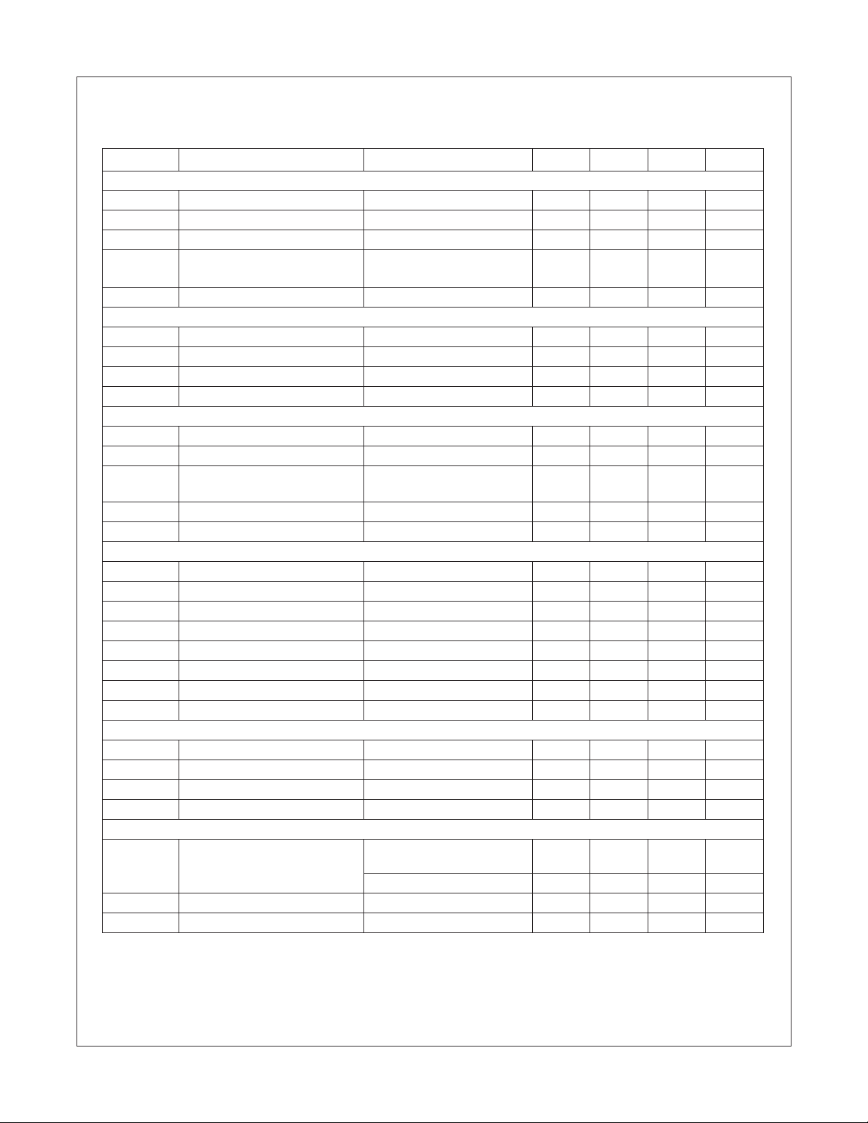
Electrical Characteristics at +3V
TA = 25°C, Vs = 3V, RL = 2kW to Vs/2, G = 2, Rf = Rg =1kW; unless otherwise noted.
Symbol Parameter Conditions Min. Typ. Max. Units
Frequency Domain Response
UGBW -3dB Bandwidth G = +1, V
BW
ss
BW
Ls
BW
0.1dBss
GBWP Gain Bandwidth Product
-3dB Bandwidth G = +2, V
Full Power Bandwidth G = +2, V
0.1dB Bandwidth
G = +2, RL = 150kW,
V
= 0.2Vpp
OUT
G = +6, V
Time Domain Response
tR, t
F
t
S
OS Overshoot V
SR Slew Rate V
Rise and Fall Time V
Settling Time to 0.1% V
= 0.2V step 12 ns
OUT
= 2V step 90 ns
OUT
= 0.2V step 1 %
OUT
= 2V step, G = -1 90
OUT
Distortion/Noise Response
HD2 2nd Harmonic Distortion V
HD3 3rd Harmonic Distortion V
THD Total Harmonic Distortion
= 1Vpp, 5MHz 50 dBc
OUT
= 1Vpp, 5MHz 50 dBc
OUT
V
= 2Vpp, 5MHz, RL =
OUT
100W, G = -1
e
X
n
TALK
Input Voltage Noise > 100kHz 17 nV/√Hz
Crosstalk FHP3230, FHP3430 at 1MHz 62 dB
DC Performance
V
dV
I
b
dI
I
IO
IO
IO
b
Input Offset Voltage 1 mV
Average Drift 5
Input Bias Current -1.8
Average Drift 4 nA/°C
Input Offset Current 0.01
PSRR Power Supply Rejection Ratio DC 100 dB
A
OL
I
S
Open-Loop Gain
DC, RL = 150W
Supply Current per Amplier 2.5 mA
Input Characteristics
R
IN
C
IN
Input Resistance 500
Input Capacitance <1.5 pF
CMIR Input Common Mode V Range -0.3 to 2 V
CMRR Common Mode Rejection Ratio DC, VCM = 0V to Vs - 1.5 95 dB
Output Characteristics
RL = 2kW to Vs/2, G = -1
V
OUT
Output Voltage Swing
RL = 150W to Vs/2, G = -1
I
OUT
I
SC
Linear Output Current ±100 mA
Short-Circuit Output Current V
= Vs/2 ±120 mA
OUT
OUT
OUT
OUT
OUT
= 0.2V
= 0.2V
= 1V
= 0.2V
pp
pp
pp
160 MHz
50 MHz
45 MHz
11.5 MHz
pp
60 MHz
50 dB
100 dB
0.05 to
2.95
0.1 to 2.9 V
FHP3130, FHP3230, FHP3430 Single, Dual, and Quad, High-Speed, 2.7V to 12V, Rail-to-Rail Ampliers
V/µs
µV/°C
µA
µA
kW
V
© 2006 Fairchild Semiconductor Corporation 4 www.fairchildsemi.com
FHP3130, FHP3230, FHP3430 Rev. 3.0.2

Electrical Characteristics at +5V
TA = 25°C, V
s
FHP3130, FHP3230, FHP3430 Single, Dual, and Quad, High-Speed, 2.7V to 12V, Rail-to-Rail Ampliers
© 2006 Fairchild Semiconductor Corporation 5 www.fairchildsemi.com
FHP3130, FHP3230, FHP3430 Rev. 3.0.2
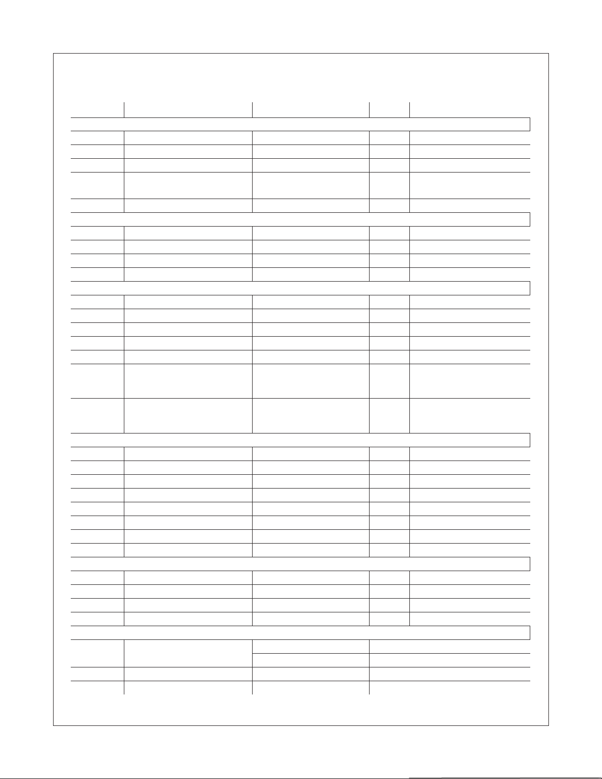
Electrical Characteristics at ±5V
TA = 25°C, Vs = ±5V, RL = 2kW to GND, G = 2, Rf = Rg =1kW; unless otherwise noted.
FHP3130, FHP3230, FHP3430 Single, Dual, and Quad, High-Speed, 2.7V to 12V, Rail-to-Rail Ampliers
© 2006 Fairchild Semiconductor Corporation 6 www.fairchildsemi.com
FHP3130, FHP3230, FHP3430 Rev. 3.0.2
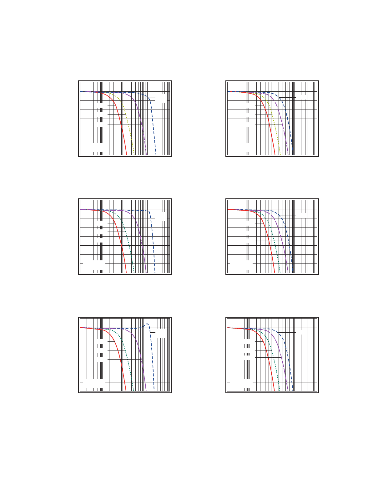
Typical Performance Characteristics
1
Normalized Gain (dB)
0.1
Frequency (MHz)
0
-1
-2
-3
-4
-5
-6
-7
1000100101
G = 10
G = 1
Rf = 0
G = 5
G = 2
Vs = ±5V
V
OUT
= 0.2V
pp
1
Normalized Gain (dB)
0.1
Frequency (MHz)
0
-1
-2
-3
-4
-5
-6
-7
1000100101
G = -1
Vs = ±5V
V
OUT
= 0.2V
pp
G = -10
G = -5
G = -2
1
Normalized Gain (dB)
0.1
Frequency (MHz)
0
-1
-2
-3
-4
-5
-6
-7
1000100101
G = 10
G = 1
Rf = 0
G = 5
G = 2
Vs = +5V
V
OUT
= 0.2V
pp
1
Normalized Gain (dB)
0.1
Frequency (MHz)
0
-1
-2
-3
-4
-5
-6
-7
1000100101
G = -1
Vs = +5V
V
OUT
= 0.2V
pp
G = -10
G = -5
G = -2
1
Normalized Gain (dB)
0.1
Frequency (MHz)
0
-1
-2
-3
-4
-5
-6
-7
1000100101
G = 10
G = 1
Rf = 0
G = 5
G = 2
Vs = +3V
V
OUT
= 0.2V
pp
1
Normalized Gain (dB)
0.1
Frequency (MHz)
0
-1
-2
-3
-4
-5
-6
-7
1000100101
G = -1
Vs = +3V
V
OUT
= 0.2V
pp
G = -10
G = -5
G = -2
T
= 25°C, Vs = 5V, RL = 2kW to Vs/2 for Vs = 5V and 3V, RL = 2kW to GND for Vs = ±5V, G = 2,
A
R
= R
= 1kW; unless otherwise noted.
f
g
Figure 1. Non-Inverting Freq. Response (±5V) Figure 2. Inverting Freq. Response (±5V)
FHP3130, FHP3230, FHP3430 Single, Dual, and Quad, High-Speed, 2.7V to 12V, Rail-to-Rail Ampliers
© 2006 Fairchild Semiconductor Corporation 7 www.fairchildsemi.com
FHP3130, FHP3230, FHP3430 Rev. 3.0.2
Figure 3. Non-Inverting Freq. Response (+5V) Figure 4. Inverting Freq. Response (+5V)
Figure 5. Non-Inverting Freq. Response (+3V) Figure 6. Inverting Freq. Response (+3V)
 Loading...