

tm
FGL40N120AND
1200V NPT IGBT
FGL40N120AND 1200V NPT IGBT
February 2008
Features
• High speed switching
• Low saturation voltage : V
• High input impedance
• CO-PAK, IGBT with FRD : t
= 2.6 V @ IC = 40A
CE(sat)
= 75ns (typ.)
rr
Description
Employing NPT technology, Fairchild’s AND series of IGBTs
provides low conduction and switching losses. The AND series
offers an solution for application such as induction heating (IH),
motor control, general purpose inverters and uninterruptible
power supplies (UPS).
Applications
Induction Heating, UPS, AC & DC motor controls and general
purpose inverters.
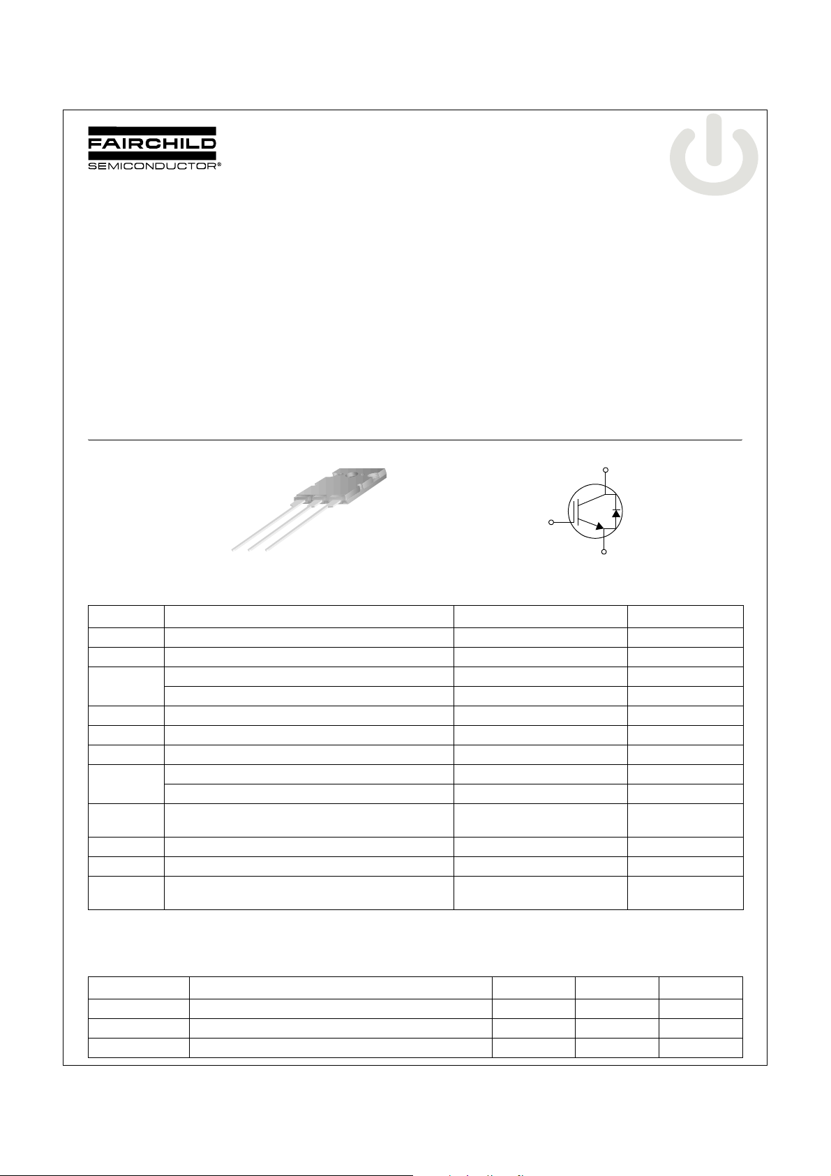
C
G
GC E
TO-264
E
Absolute Maximum Ratings
Symbol Parameter FGL40N120AND Units
V
CES
V
GES
I
C
I
CM(1)
I
F
I
FM
P
D
SCWT
T
J
T
STG
T
L
Notes:
(1) Pulse width limited by max. junction temperature
Collector-Emitter Voltage 1200 V
Gate-Emitter Voltage ±25 V
Collector Current @TC = 25°C64 A
Collector Current @T
Pulsed Collector Current 160 A
Diode Continuous Forward Current @TC = 100°C40 A
Diode Maximum Forward Current 240 A
Maximum Power Dissipation @TC = 25°C 500 W
Maximum Power Dissipation @T
Short Circuit Withstand Time,
V
= 600V, VGE = 15V, TC = 125°C
CE
Operating Junction Temperature -55 to +150 °C
Storage Temperature Range -55 to +150 °C
Maximum Lead Temp. for Soldering
Purposes, 1/8” from Case for 5 seconds
= 100°C40 A
C
= 100°C 200 W
C
10 µs
300 °C
Thermal Characteristics
Symbol Parameter Typ. Max. Units
R
(IGBT) Thermal Resistance, Junction-to-Case -- 0.25 °C/W
θJC
(DIODE) Thermal Resistance, Junction-to-Case -- 0.7 °C/W
R
θJC
R
θJA
©2008 Fairchild Semiconductor Corporation 1 www.fairchildsemi.com
FGL40N120AND Rev. A2
Thermal Resistance, Junction-to-Ambient -- 25 °C/W

Package Marking and Ordering Information
Device Marking Device Package Reel Size Tape Width Quantity
FGL40N120AND FGL40N120AND TO-264 - - 25
FGL40N120AND 1200V NPT IGBT
Electrical Characteristics of the IGBT T
= 25°C unless otherwise noted
C
Symbol Parameter Conditions Min. Typ. Max. Units
Off Characteristics
BV
CES
BV
CES
∆T
J
I
CES
I
GES
On Characteristics
V
GE(th)
V
CE(sat)
Dynamic Characteristics
C
ies
C
oes
c
res
Switching Characteristics
t
d(on)
t
r
t
d(off)
t
f
E
on
E
off
E
ts
t
d(on)
t
r
t
d(off)
t
f
E
on
E
off
E
ts
Q
g
Q
ge
Q
gc
Collector-Emitter Breakdown Voltage VGE = 0V, IC = 1mA 1200 -- -- V
/
Temperature C oefficient of Breakdown
Voltage
Collector Cut-Off Current VCE = V
G-E Leakage Current VGE = V
G-E Threshold Voltage IC = 250µA, VCE = V
Collector to Emitter
Saturation Voltage
Input Capacitance
Output Capacitance -- 370 -- pF
V
= 0V, IC = 1mA -- 0.6 -- V/°C
GE
, VGE = 0V -- -- 1 mA
CES
, VCE = 0V -- -- ±250 nA
GES
GE
I
= 40A, VGE = 15V -- 2.6 3.2 V
C
= 40A, VGE = 15V,
I
C
T
= 125°C
C
= 64A, VGE = 15V -- 3.15 -- V
I
C
3.5 5.5 7.5 V
-- 2.9 -- V
-- 3200 -- pF
V
= 30V, VGE = 0V
CE
f = 1MHz
Reverse Transfer Capacitance -- 125 -- pF
Turn-On Delay Time
-- 15 -- ns
Rise Time -- 20 -- ns
Turn-Off Delay Time -- 110 -- ns
Fall Time -- 40 80 ns
Turn-On Switching Loss -- 2.3 3.45 mJ
V
= 600V, IC = 40A,
CC
R
= 5Ω, VGE = 15V,
G
Inductive Load, T
= 25°C
C
Turn-Off Switching Loss -- 1.1 1.65 mJ
Total Switching Loss -- 3.4 5.1 mJ
Turn-On Delay Time
-- 20 -- ns
Rise Time -- 25 -- ns
Turn-Off Delay Time -- 120 -- ns
Fall Time -- 45 -- ns
Turn-On Switching Loss -- 2.5 -- mJ
V
= 600V, IC = 40A,
CC
R
= 5Ω, VGE = 15V,
G
Inductive Load, T
= 125°C
C
Turn-Off Switching Loss -- 1.8 -- mJ
Total Switching Loss -- 4.3 -- mJ
Total Gate charge
V
= 600V, IC = 40A,
Gate-Emitter Charge -- 25 38 nC
Gate-Collector Charge -- 130 195 nC
V
CE
GE
= 15V
-- 220 330 nC
FGL40N120AND Rev. A2
2 www.fairchildsemi.com
FGL40N120AND 1200V NPT IGBT
Electrical Characteristics of DIODE T
= 25°C unless otherwise noted
C
Symbol Parameter Test Conditions Min. Typ. Max. Units
I
= 40A TC = 25°C--3.24.0
V
FM
t
rr
I
rr
Q
rr
Diode Forward Voltage
Diode Reverse Recovery Time
Diode Peak Reverse Recovery
Current
Diode Reverse Recovery Charge
F
= 40A,
I
F
di/dt = 200A/µs
= 125°C-- 2.7 --
T
C
T
= 25°C--75112
C
= 125°C -- 130 --
T
C
T
= 25°C-- 812
C
= 125°C-- 13 --
T
C
T
= 25°C -- 300 450
C
= 125°C -- 845 --
T
C
V
nS
A
nC
FGL40N120AND Rev. A2
3 www.fairchildsemi.com
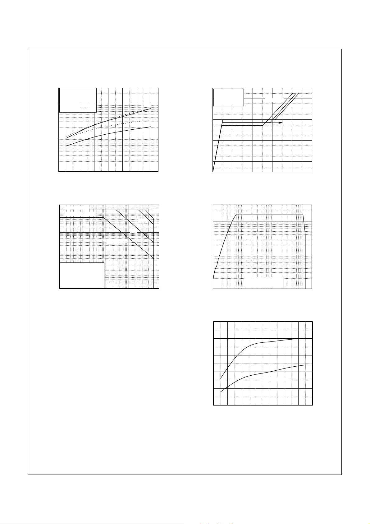
Typical Performance Characteristics
Figure 1. Typical Output Characteristics Figure 2. Typical Saturation Voltage
Characteristics
300
TC = 25°C
250
200
[A]
C
150
100
Collector Current, I
50
20V
17V
15V
12V
VGE = 10V
[A]
Collector Current, I
150
120
C
Common Emitter
VGE = 15V
TC = 25°C
TC = 125°C
90
60
30
FGL40N120AND 1200V NPT IGBT
0
0246810
Collector-Emitter Voltage, VCE [V]
0
0246
Collector-Emitter Voltage, VCE [V]
Figure 3. Saturation Voltage vs. Case Figure 4. Load Current vs. Frequency
Temperature at Variant Current Level
5
Common Emitte r
VGE = 15V
[V]
4
CE
3
2
Collector-Emitter Voltage, V
1
25 50 75 100 125
Case Temperature, TC [°C]
Figure 5. Saturation Voltage vs. V
20
Common Emitter
TC = 25°C
16
[V]
CE
80A
40A
IC = 20A
GE
80
70
60
50
40
30
Load Current [A]
20
Duty cycle : 50%
10
TC = 100°C
Power Dissipation = 100W
0
0.1 1 10 100 1000
VCC = 600V
Load Current : peak of square wave
Frequency [ kHz]
Figure 6. Saturation Voltage vs. V
20
Common Emitter
TC = 125°C
16
[V]
CE
GE
12
8
4
Collector-Emitter Voltage, V
0
048121620
FGL40N120AND Rev. A2
80A
40A
IC = 20A
Gate-Emitter Voltage, VGE [V]
12
8
4
Collector-Emitter Voltage, V
0
048121620
80A
40A
IC = 20A
Gate-Emitter Voltage, VGE [V]
4 www.fairchildsemi.com
Typical Performance Characteristics (Continued)
Figure 7. Capacitance Characteristics Figure 8. Turn-On Characteristics vs. Gate
Resistance
6000
5000
4000
3000
2000
Capacitance [pF]
1000
0
Ciss
Coss
Crss
110
Collector-Emitter Voltage, VCE [V]
Figure 9. Turn-Off Characteristics vs. Figure 10. Switching Loss vs. Gate Resistance
Gate Resistance
Common Emitter
VGE = 0V, f = 1MHz
TC = 25°C
100
tr
Switching Time [ns]
10
td(on)
0 10203040506070
Common Emitter
VCC = 600V, VGE = ±15V
IC = 40A
TC = 25°C
TC = 125°C
Gate Resistance, RG [Ω]
FGL40N120AND 1200V NPT IGBT
Common Emitter
VCC = 600V, VGE = ±15V, IC = 40A
1000
TC = 25°C
TC = 125°C
100
Switching Time [ns]
10
0 10203040506070
Gate Resistance, RG [Ω]
td(off)
tf
Common Emitter
VCC = 600V, VGE = ±15V
IC = 40A
TC = 25°C
10
TC = 125°C
Switching Loss [mJ]
1
0 10203040506070
Gate Resistance, RG [Ω]
Eon
Eoff
Figure 11. Turn-On Characteristics vs. Figure 12. Turn-Off Characteristics vs.
Collector Current Collector Current
20 30 40 50 60 70 80
FGL40N120AND Rev. A2
5 www.fairchildsemi.com
Typical Performance Characteristics (Continued)
Figure 13. Switching Loss vs. Collector Current Figure 14. Gate Charge Characteristics
Common Emitter
VGE = ±15V, RG = 5Ω
TC = 25°C
10
1
TC = 125°C
Eon
Eoff
Switching Loss [mJ]
0.1
20 30 40 50 60 70 80
Collector Curr en t , IC [A]
Figure 15. SOA Characteristics Figure 16. Turn-Off SOA
16
Common Emitter
RL = 15Ω
14
TC = 25°C
12
[V]
GE
10
8
6
4
Gate-Emitter Voltage, V
2
0
0 50 100 150 200 250
Vcc = 200V
400V
Gate Charge, Qg [nC]
600V
FGL40N120AND 1200V NPT IGBT
Ic MAX (Pulsed)
100
Ic MAX (Continuous)
10
DC Operation
1
Single Nonrepetitive
0.1
Collector Current, Ic [A]
Pulse Tc = 25oC
Curves must be derated
linearly with increase
in temperature
0.01
0.1 1 10 100 1000
Collector - Emitter Voltage, VCE [V]
1ms
100µs
50µs
100
[A]
C
10
Collector Current, I
Safe Operating Area
1
1 10 100 1000
VGE = 15V, TC = 125oC
Collector-Emitter Voltage, VCE [V]
Figure 17. Forward Characteristics Figure 18. Reverse Recovery Current
10
8
6
4
2
FGL40N120AND Rev. A2
0
0 10203040506070
6 www.fairchildsemi.com
Typical Performance Characteristics (Continued)
Figure 19. Stored Charge Figure 20. Reverse Recovery Time
100
400
FGL40N120AND 1200V NPT IGBT
90
[ns]
rr
80
70
60
di/dt = 200A/µs
di/dt = 100A/µs
Reverse Recovery Time , t
50
0 10203040506070
Forward Current , IF [A]
Figure 21. Transient Thermal Impedance of IGBT
1
0.5
0.1
0.2
0.1
0.05
0.01
Thermal Response [Zthjc]
0.02
0.01
single pulse
1E-3
1E-5 1E-4 1E-3 0.01 0.1 1 10
[nC]
rr
300
200
100
Stored Recovery Charge , Q
0
0 10203040506070
Rectangular Pu lse Du rati on [sec]
di/dt = 200A/µs
di/dt = 100A/µs
Forward Current , IF [A]
Pdm
Pdm
t1
t1
t2
t2
Duty factor D = t1 / t2
Duty factor D = t1 / t2
Peak Tj = Pdm
Peak Tj = Pdm
×
Zthjc + T
×
Zthjc + T
C
C
FGL40N120AND Rev. A2
7 www.fairchildsemi.com

Mechanical Dimensions
FGL40N120AND 1200V NPT IGBT
FGL40N120AND Rev. A2
8 www.fairchildsemi.com

TRADEMARKS
The following includes registered and unregistered trademarks and service marks, owned by Fairchild Semiconductor and/or its global
subsidianries, and is not intended to be an exhaustive list of all such trademarks.
®
ACEx
Build it Now™
CorePLUS™
CROSSVOLT™
CTL™
Current Transfer Logic™
EcoSPARK
EZSWITCH™ *
™
Fairchild
®
®
Fairchild Semiconductor
FACT Quiet Series™
®
FACT
®
FAST
FastvCore™
FlashWriter
®
*
®
FPS™
®
FRFET
Global Power Resource
Green FPS™
Green FPS™ e-Series™
GTO™
i-Lo™
IntelliMAX™
ISOPLANAR™
MegaBuck™
MICROCOUPLER™
SM
FGL40N120AND 1200V NPT IGBT
* EZSWITCH™ and FlashWriter
®
are trademarks of System General Corporation, used under license by Fairchild Semiconductor.
DISCLAIMER
FAIRCHILD SEMICONDUCTOR RESERVES THE RIGHT TO MAKE CHANGES WITHOUT NOTICE TO ANY PRODUCTS HEREIN TO
IMPROVE RELIABILITY, FUNCTION, OR DESIGN. FAIRCHILD DOES NOT ASSUME ANY LIABILITY ARISING OUT OF THE
APPLICATION OR USE OF ANY PRODUCT OR CIRCUIT DESCRIBED HEREIN; NEITHER DOES IT CONVEY ANY LICENSE UNDER ITS
PATENT RIGHTS, NOR THE RIGHTS OF OTHERS. THESE SPECIFICATIONS DO NOT EXPAND THE TERMS OF FAIRCHILD’S
WORLDWIDE TERMS AND CONDITIONS, SPECIFICALLY THE WARRANTY THEREIN, WHICH COVERS THESE PRODUCTS.
LIFE SUPPORT POLICY
FAIRCHILD’S PRODUCTS ARE NOT AUTHORIZED FOR USE AS CRITICAL COMPONENTS IN LIFE SUPPORT DEVICES OR
SYSTEMS WITHOUT THE EXPRESS WRITTEN APPROVAL OF FAIRCHILD SEMICONDUCTOR CORPORATION.
As used herein:
1. Life support devices or systems are devices or systems which,
(a) are intended for surgical implant into the body or (b)
support or sustain life, and (c) whose failure to perform when
properly used in accordance with instructions for use provided
2. A critical component in any component of a life support, device
or system whose failure to perform can be reasonably
expected to cause the failure of the life support device or
system, or to affect its safety or effectiveness.
in the labeling, can be reasonably expected to result in a
significant injury to the user.
PRODUCT STATUS DEFINITIONS
Definition of Terms
FGL40N120AND Rev. A2
Rev. I33
9 www.fairchildsemi.com
 Loading...